Rigid-Flex PCB Design: Benefits, Applications, Routing, and Manufacturing Guide
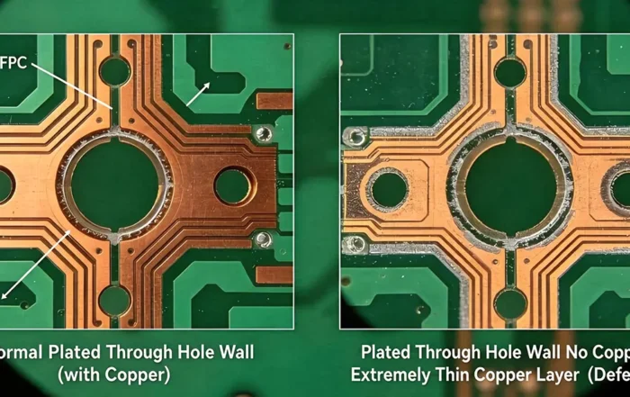

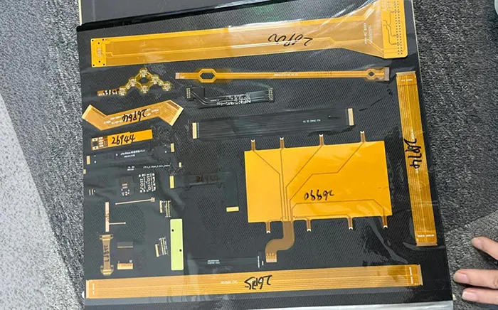
Combining all the characteristics of flexible circuits with rigid circuit boards that fully leverage high-density interconnect (HDI) technology represents a major technological breakthrough of our time.
This design successfully avoids the need for board-to-board stacking connectors or typical flexible circuits.
Anyone who has attempted to mate a flexible circuit with a stacking connector knows that this is a bottleneck in the entire process—this “blind mating” operation is extremely demanding in terms of manual dexterity, and even the slightest misalignment can result in connector damage.
The rigid-flex design combines the strengths of both approaches while also incorporating their weaknesses.
First, if a team adopts this approach, it indicates that they place great importance on all possible forms of integration.
Although the industry highly values both technologies, the rigid PCB sector remains larger and receives broader market recognition.
Independent Applications of Flexible Circuits
Designing flexible printed circuits (FPCs) involves more than selecting different materials.
Engineers must create more robust structures than those used in conventional PCBs and incorporate additional design tolerances to accommodate manufacturing and operational requirements.
One key reason for this is the use of various types of material stacks during the manufacturing process. In most cases, flexible boards also include rigid sections for mounting connectors.
Designers can extend these reinforced areas to support components such as electrostatic discharge (ESD) protection devices, light-emitting diodes (LEDs), and microphones.
This approach provides greater design flexibility while accommodating a wider range of functional components.
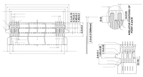
Figure 1 Printed connector with staggered pins. Image source Hirose
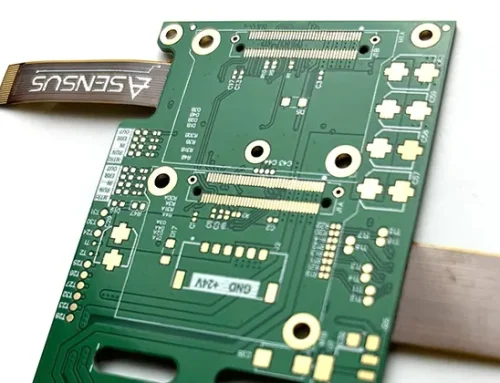
Zero Insertion Force (ZIF) connectors provide a good example because designers can print them directly onto flexible circuit boards.
With this method, a reinforcing rib is located at the end of the flexible circuit board to support the pins.
Insert the reinforcing rib into the mating connector, then press down the connector lever to lock the flexible circuit board’s tail fin securely in place.
Whether the board is purely flexible or a rigid-flex board, assembly using ZIF connectors is simpler than using stacked connectors.
Examples of Rigid-Flex Combination Applications
Flexible circuit boards have a wide range of applications. For example, in wearable technology designs, attaching a stiffener to the center of a flexible board creates circular “islands.”
Components cluster like small communities atop these stiffener islands, while the circuitry runs around them. Rigid areas are integrated into augmented reality headsets and positioned around the ears and other locations.
Applications such as eye tracking require more complex design solutions. No substrate material can make a 12-layer PCB completely flexible.
Designers can instead consider semi-flexible boards, while rigid-flex PCBs provide the advantage of supporting complex routing with up to a dozen layers in localized areas where higher interconnect density is required.
In addition, designers can extend a flexible core from the rigid section to carry a specific group of signal lines.
A common configuration involves embedding three flexible layers within an 8-layer or 10-layer board.
Designers also use odd-layer stackups in many rigid-flex PCB applications. For example, they can start the stackup with a single-sided flexible layer to maximize overall flexibility.
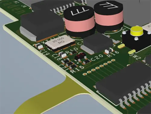
Figure 2 Note the radius at which the flexible core extends from the rigid section this design, combined with epoxy beads, relieves stress on the flexible board tail. Image credit Cadence
Advantages of Combining Rigidity and Flexibility
The stacking of polyimide core materials enables the rigid sections to support double-sided component mounting.
Typically, the size requirements for such products are “the smaller, the better”; since we have opted for this cutting-edge solution, it indicates that the design challenges we face must be highly complex.
Consequently, ball grid array (BGA) packages and various related micro-components come into play.
Larger BGA packages often rely on smaller BGAs to support auxiliary functions.
Designers can position these smaller BGAs in different rigid sections throughout the rigid-flex PCB to optimize space and circuit layout.
Continuing with the augmented reality (AR) theme, one use case involves flexible antenna extensions, where the antenna’s position and orientation are integral to the product’s overall profile.
The radio chip is located on the rigid-flex circuit board, so the remote antenna forms part of the flexible attachment. Such special cases may also require dedicated electromagnetic interference (EMI) shielding layers.
Designers should solder the EMI suppression material to a dedicated ground plane designed specifically for this purpose.
The manufacturing process applies the EMI film after all other layers are completed, so designers must cut a series of small notches into the cover film to expose the grounding areas.
During the design phase, they should account for these features and incorporate them into the additional physical layers.
Pursuing Coexistence
Coexistence is always the top priority, especially in the early stages of design. Once the design team identifies a viable solution, they can remove selected safeguards to determine whether the design still meets the required standards.
This is what we call lean design—reducing the number of components through iteration.
In practice, however, the early design stages may actually require additional filters or other improvements, leading to an increase in the number of components.
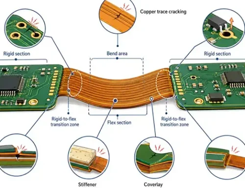
If you are familiar with flexible PCB manufacturing, you know that the transition from rigid to flexible areas is one of the key challenges. The same applies to exiting the rigid area.
Polyimide extends throughout the rigid area and branches out into the flexible section to reach its destination.
These destinations can be entirely new circuit boards with a structure identical to the main rigid board area, or they can utilize common solutions such as stiffeners and connectors.
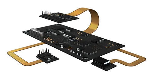
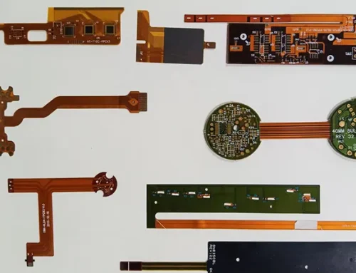
Figure 3 Segmented electronic components offer endless options compared to rigid flex designs. Image source Cadence
We cannot have a 4-layer board in one section and a 10-layer board in another within the same design.
Since all sections are laminated simultaneously, like a “layer cake,” the lamination process for all multi-layer rigid sections must be completely consistent; only at the lead-out ends of the flexible board can we apply various conventional flexible board geometries.
Designers often install a connector at the end of the flexible section.
However, they can also integrate virtually any combination of components supported by a single-sided flexible PCB.
Routing Controlled-Impedance Traces on Rigid-Flex PCBs
This scenario often arises: we want to extend differential pairs from a rigid region to a flexible region. Suppose we use a 3-layer flexible PCB with a ground plane on the outer layer, with the signal traces located within a Faraday cage; this is a prerequisite for achieving controlled impedance.
Placing the signal traces at the center of the flexible stackup, within the neutral layer, reduces the stress on the traces. In contrast, a two-layer structure places the traces under severe tension or compression when the board bends.
We aim to maintain consistent impedance in the rigid region from the inside out.
Specifically, designers maintain this structure by extending a grid alongside the traces on the outer layer of the polyimide.
Beyond the controlled-impedance routing area, the outer layer of the flexible board is more likely to use a solid ground plane; while this sacrifices some flexibility, it provides a more stable upper and lower reference plane for the transmission lines.
If you want to minimize issues caused by connector-specific failure modes and assembly challenges, rigid-flex boards may be a good choice.
Although they require a greater investment of time in both layout planning and adapting to manufacturer limitations, the advantages in assembly more than offset the initial investment.
Improved reliability is just the icing on the cake; the key is to achieve the stability of a rigid board and the flexibility of a flexible board simultaneously.
Conclusion
Rigid-flex PCBs combine the structural stability of rigid boards with the routing flexibility of flexible circuits, providing an effective solution for compact, high-density electronic products.
By eliminating many traditional board-to-board connectors, they simplify assembly, reduce potential failure points, and improve overall system reliability.
These advantages make rigid-flex technology particularly valuable for applications such as wearable devices, augmented reality systems, medical electronics, aerospace equipment, and other products where space, weight, and durability are critical.
Successful rigid-flex designs, however, require careful planning from the earliest stages of development.
Designers must consider stack-up architecture, transition zones between rigid and flexible sections, controlled-impedance routing, stiffener placement, EMI shielding, and manufacturing constraints as part of a unified design strategy.
Close collaboration with the PCB manufacturer is equally important to ensure that the chosen materials, lamination process, and fabrication capabilities align with the design requirements.
Although rigid-flex PCBs demand greater engineering effort than conventional rigid or flexible boards alone, the long-term benefits often outweigh the additional complexity.
With thoughtful design and proper manufacturing practices, rigid-flex technology enables highly integrated electronic products that deliver superior reliability, easier assembly, and exceptional mechanical performance in demanding operating environments.