
Multilayer FPC Layer Registration: How to Ensure Accurate Layer-to-Layer Alignment
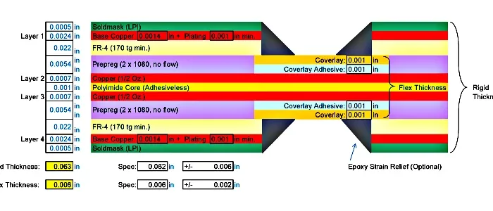
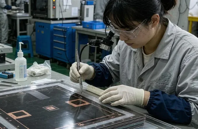
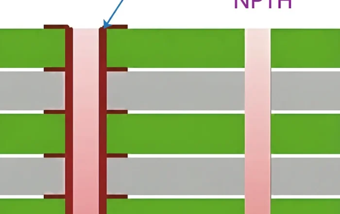
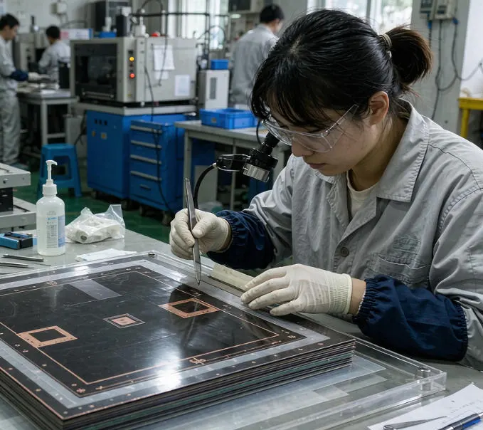
Additionally, multilayer FPC layer registration is the control of layer-to-layer positional accuracy during stack-up, lamination, and drilling. Meanwhile, it is measured from fiducials and target pads, and is usually held to ±25–50 µm on standard builds and ±10–25 µm on high-density ones. For example, stable materials, scaled artwork, and controlled lamination make the result repeatable.
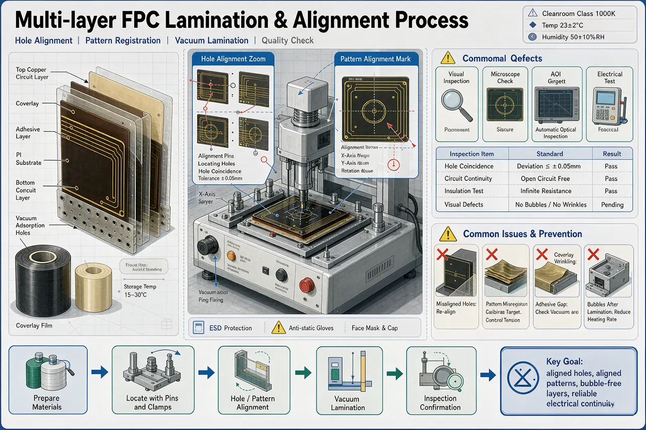
Multi-layer FPC Lamination & Alignment Process
In addition, see also High-Reliability Flexible Circuits for High-End Applications for related specifications.
As a result, see also Rigid-Flex PCB Technology for related specifications.
However, see also PCB Manufacturing FAQ for related specifications.
In practice, this guide defines registration accuracy with real numbers, explains where alignment drifts, and shows how to measure and compensate it. Next, the focus stays on three-or-more-layer flex and rigid-flex builds, where every extra lamination cycle adds error.
What Is Layer Registration Accuracy in a Multilayer FPC?
Consequently, layer registration accuracy is the measured offset between a feature on one layer and its target position on another layer. Moreover, common metrics are pad-to-via offset, pad-to-pad offset, and image-to-image offset between inner layers.
In particular, tolerance is stated in micrometres (µm) or mils, where 1 mil equals 25.4 µm. However, it is a stack-up allowance, not a single machine specification. Therefore, imaging, lamination, drilling, and coverlay bonding each consume part of the budget.
| Build type | Typical registration tolerance | Typical process |
|---|---|---|
| Standard 4–6 layer FPC | ±50 µm | Mechanical drill, 100 µm line/space |
| Fine-line 6–8 layer FPC | ±25 µm | LDI imaging, laser via |
| High-density / rigid-flex | ±10–25 µm | Multiple lamination cycles, thin PI |
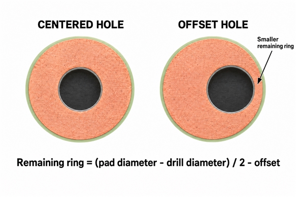
A simple design rule helps: keep the pad annular ring at least 1.5 times the expected tolerance, and never treat the full tolerance as design margin.
Why Registration Is a Multilayer-Specific Problem
A single-sided FPC has one conductor layer, so alignment is mainly coverlay-to-copper. Therefore, a double-sided FPC adds one drill step. A Multilayer Flex PCB with three or more conductor layers adds inner-layer imaging, oxide treatment, and at least one vacuum lamination cycle.
Each extra cycle brings another round of heat, pressure, and resin flow. Shrinkage therefore compounds. High-density digital and High-Frequency Rigid-Flex PCB designs push this further, because impedance and stub control both depend on layer alignment.
Six Root Causes of Layer Shift
1. Material dimensional stability. Polyimide absorbs moisture and expands with heat. An uncontrolled bake and lamination cycle can move features by well over 100 µm across a large panel.
2. Lamination resin flow. Adhesive softens and flows under pressure. Layers may slide sideways before the resin gels, especially on large panels.
3. Artwork scaling. Film stretch, plotter drift, and thermal expansion during exposure change image size. A 0.02% scale error equals 60 µm on a 300 mm panel.
4. Exposure and development drift. Lamp intensity fall-off and developer concentration change line width and effective image position.
5. Drill and via offset. Mechanical drilling references the outer layer. Inner pads must sit inside the drill allowance, or the via will clip the target pad.
6. Coverlay opening offset. The coverlay is bonded after drilling, so its openings can shift relative to pads even when inner layers are perfect.
When inner pads are exposed or partially covered, the choice of inner-layer pad protection methods for FPC also affects how much misregistration a design can absorb before reliability drops.
Registration Checkpoints in the Process Flow
Registration is controlled step by step, not inspected only at the end. Add a checkpoint at each stage of Multi-layer FPC manufacturing:
- Inner-layer imaging. Expose every layer from the same scaled artwork set, then measure the panel-border coupon.
- Development and etch. Check line width and etch factor, because both shift apparent feature position.
- Oxide treatment. Brown or black oxide controls adhesion and resin flow. Uniform oxide reduces layer slip.
- Vacuum lamination. Program ramp rate, pressure, and cooling, and cool under pressure to lock alignment.
- Drilling and via formation. Use X-ray targets and global panel fiducials, then verify via-to-pad offset on the first panel.
- Coverlay and surface finish. Check opening-to-pad offset before final cure.
- Shielding. On dense builds, an EMI shielding film is added after coverlay. The EMI Shielding Method guide covers the extra alignment step this introduces.
How to Measure Layer Registration
Use more than one method, because each one catches a different failure mode.
- Fiducials and registration marks. Three or four global marks on the panel border give the coordinate reference. Add per-layer targets for inner-layer checks.
- X-ray via-to-pad alignment. Non-destructive and fast. Measure a fixed sample per panel or per lot.
- AOI. Automated optical inspection flags pad and opening offsets on outer layers. It is fast but blind to buried layers.
- Overlay coupons. Place a coupon in the panel border that repeats the critical stack, then cross-section it and measure directly.
- Cross-sections. The reference method for buried vias and annular ring. Use it to calibrate the non-destructive methods.
Record every measurement against the panel ID. Registration data that cannot be traced back to a lot has little value during a customer audit.
Design Compensation Tactics
Compensation is usually cheaper than tightening every process step.
- Artwork scaling. Apply a scale factor per layer, typically 0.02–0.05%, based on measured shrink instead of guesswork. Scale X and Y separately when the material is anisotropic, since polyimide often shrinks differently in machine and cross directions.
- Panel border marks. Add global fiducials plus one target per layer. This costs little space and makes X-ray checks possible.
- Shrinkage compensation. Measure a test panel through the full cycle, then feed the result back into the artwork. Repeat after any material or press program change.
- Tolerance stack-up. Sum imaging, lamination, drilling, and coverlay error. If the total exceeds the pad allowance, tighten the dominant term first.
- Pad and annular ring design. Size pads for worst-case offset, not the nominal value. Teardrops help on high-layer-count builds where drill breakout risk rises.
For mixed constructions, the same rules apply in Rigid-flex PCB manufacturing, but the rigid section usually adds its own drill and lamination tolerance.
Drill After Lamination vs Laser Via
Through vias in multilayer FPC are normally drilled after lamination. The outer layer becomes the reference, so inner-layer pads must carry the full drill allowance.
Laser vias are formed layer by layer or after bonding, depending on the structure. Depth control and pad capture become the critical parameters. Structures such as a Blind Slot need dedicated depth control and energy settings, and they leave less margin for registration error.
Registration also affects insulation spacing. When pads and vias sit near the edge of the drill allowance, the risk of CAF Failure in Multilayer FPCBs rises under bias and humidity. Keep electrical clearance independent of the registration budget.
Troubleshooting Matrix
| Symptom | Likely cause | Corrective action |
|---|---|---|
| Uniform shift in one direction | Artwork scale error or film stretch | Re-measure coupon, rescale artwork |
| Random shift between panels | Lamination slip or uneven pressure | Check press flatness, slow the ramp, cool under pressure |
| Via clipping inner pad | Drill offset or undersized pad | Recalibrate drill, add annular ring margin |
| Coverlay opening off pad | Coverlay tooling stretch or misalignment | Verify coverlay artwork, use pinned lamination |
| Shift only on outer layers | Exposure or development drift | Recalibrate lamp, check developer chemistry |
| Shift grows with each cycle | Shrink accumulation per lamination cycle | Compensate per cycle, review material lot |
Acceptance Sampling and Traceability
Set an AQL level per customer requirement, then apply it to registration measurements rather than visual inspection alone. Sample the first panel of every lot, then at a fixed interval.
Track results on SPC charts. A drifting mean predicts failure before scrap appears. Keep the artwork scale factor, press program, and material lot in the same record, so any shift can be traced to its cause.
Gekun builds multilayer and rigid-flex FPCs with LDI imaging, X-ray registration checks, and per-lot traceability. Share your stack-up and tolerance target for a build review.
FAQ
What is a typical layer registration tolerance for multilayer FPCs? Standard 4–6 layer builds with mechanical drilling hold about ±50 µm. Fine-line builds with LDI imaging hold ±25 µm. High-density and rigid-flex builds with laser vias reach ±10–25 µm.
What causes layer misregistration in multilayer flex circuits? The main causes are material expansion from moisture and heat, resin flow during lamination, artwork scaling errors, exposure and development drift, drill offset, and coverlay opening offset.
How is layer registration measured? Engineers combine panel fiducials, X-ray via-to-pad checks, AOI on outer layers, border overlay coupons, and cross-sections. Cross-sections calibrate the faster non-destructive methods.
Should vias be drilled before or after lamination? Through vias in multilayer FPC are normally drilled after lamination, using the outer layer as reference. Blind laser vias are formed with depth control instead, which changes how much registration allowance the inner pads need.
Related Posts
- Multi-layer FPC Manufacturing Process: Cutting to Testing — Related article
- EMI Shielding Method for FPC and Flex Circuits Guide — Related article
- High-Frequency Rigid-Flex PCB Manufacturing — Related article
- Inner-Layer Pad Protection Methods for FPC — Related article
- Optimizing Blind Slot Multilayer Flexible PCB Manufacturing — Related article
- PCB Lamination Process Explained: From Rigid Boards to Flexible PCB Manufacturing