AOI and electrical testing for flex PCB
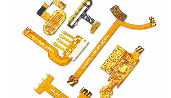
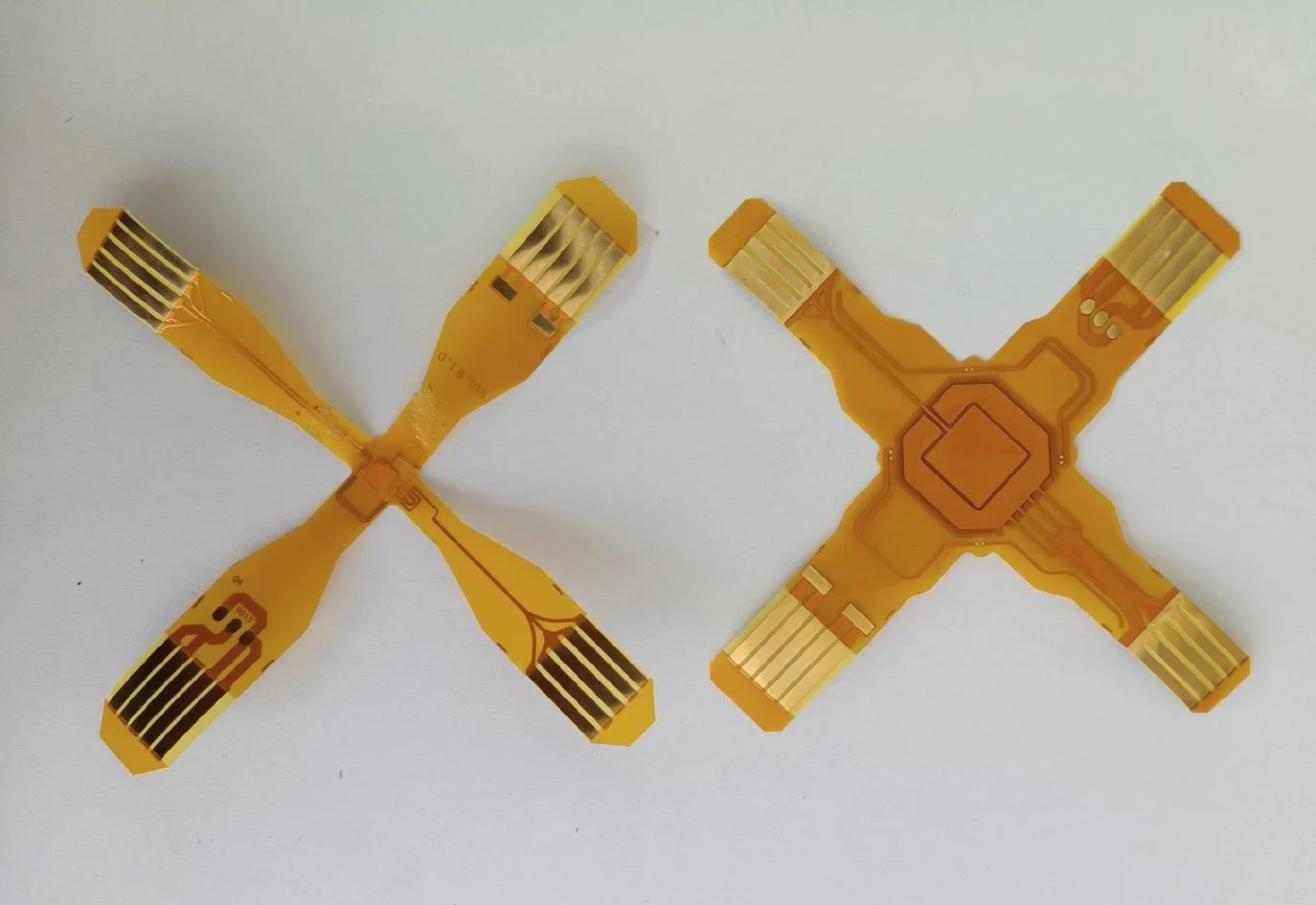
Flexible printed circuit boards (Flex PCBs) have become essential in modern electronics, enabling compact designs, dynamic movement, and lightweight assemblies.
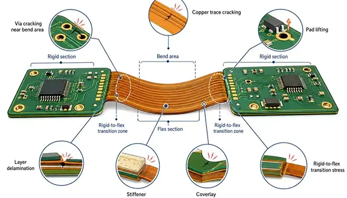
Yet, the very properties that make them attractive—thin copper, flexible substrates, and mechanical compliance—also introduce failure mechanisms that differ fundamentally from rigid PCBs.
Because of this, traditional inspection approaches are no longer sufficient. Ensuring quality in flex circuits requires a dual-layer strategy that combines visual inspection (AOI) with electrical validation.
1. Why Flex PCBs Fail Differently (And Why Testing Must Adapt)
A rigid PCB is designed to remain stable throughout its lifecycle, experiencing minimal deformation. In contrast, a flex PCB is expected to bend, twist, and sometimes endure thousands of dynamic cycles.
This continuous mechanical stress directly affects the integrity of copper traces and material interfaces.
Copper in flex circuits is typically much thinner—often down to 9 µm—making it more vulnerable to fatigue. Over time, repeated bending can initiate micro-cracks that are invisible to the naked eye but capable of causing intermittent electrical failure.
At the same time, the layered structure of polyimide and copper can separate under stress, leading to delamination or pad lifting.
Unlike rigid boards, where failures are often immediate and detectable, flex PCB failures tend to be latent and intermittent. A circuit may pass initial inspection but fail later in the field, especially in applications involving motion or vibration.
Industry standards such as IPC-2223 emphasize that mechanical reliability is a dominant factor in flex circuit performance.
This reality leads to a critical conclusion: relying on a single inspection method—whether visual or electrical—is not enough.
The solution is a dual-layer quality strategy, where Automated Optical Inspection identifies physical defects, while electrical testing verifies actual circuit functionality.
2. What Makes Flex PCB Testing More Challenging?
Testing flex PCBs is inherently more complex because the material itself is not dimensionally stable.
Polyimide substrates, often ranging from 12.5 to 50 µm in thickness, can stretch or deform slightly during manufacturing. Even small variations can affect alignment and inspection accuracy.
This instability becomes especially problematic in high-density designs. Modern flex circuits frequently use fine pitch geometries below 75 µm, where even a minor deviation can create a short or open circuit.
At the same time, the flexible panel may not remain perfectly flat during inspection, introducing further uncertainty in imaging systems.
Another layer of complexity comes from hidden defects. A trace that appears intact under inspection may already contain micro-fractures that only propagate under bending or thermal cycling.
These defects are particularly dangerous because they escape early detection and only reveal themselves during real-world operation.
In this context, neither AOI nor electrical testing alone can provide full coverage. AOI struggles with deformation and hidden defects, while electrical testing cannot identify the physical root cause of a failure.
This is why the two methods must work together, forming a complementary system rather than independent processes.
3. AOI for Flex PCB: More Than Just Visual Inspection
Automated Optical Inspection remains a cornerstone of PCB quality control, but its application in flex circuits requires careful adaptation. Unlike rigid boards, flex PCBs introduce variability that challenges conventional AOI systems.
In practice, AOI is highly effective at detecting visible manufacturing defects. It can identify trace discontinuities caused by over-etching, misalignment of coverlay layers, and deformation of pads after lamination.
For assembled flex PCBs, it also plays a key role in spotting solder-related issues such as bridging or insufficient wetting.
However, the flexible nature of the substrate complicates inspection. Slight warping or stretching can shift the circuit pattern enough to trigger false defect calls.
Conversely, overly tolerant settings may allow real defects to pass undetected. This balance between sensitivity and accuracy is far more difficult to achieve than in rigid PCB inspection.
To overcome these challenges, advanced AOI systems for flex applications increasingly rely on adaptive algorithms and multi-point alignment techniques.
Instead of assuming a fixed geometry, the system dynamically adjusts to the actual shape of the panel.
In more advanced setups, 3D AOI is used to evaluate solder height and volume, adding another dimension of inspection capability.
The key insight is that AOI is not a plug-and-play solution for flex PCBs. It must be engineered specifically for flexible materials and continuously optimized to maintain accuracy.
4. Electrical Testing: The Only Way to Catch Invisible Defects
While AOI focuses on what can be seen, electrical testing addresses what truly matters: whether the circuit functions correctly. This distinction becomes especially important in flex PCBs, where many critical defects are not visually detectable.
Electrical testing methods vary depending on production volume and application.
Flying probe systems are commonly used in prototyping and low-volume manufacturing because they require no dedicated fixtures and can adapt quickly to design changes.
In high-volume production, fixture-based testing provides speed and repeatability, making it more suitable for mass manufacturing.
Regardless of the method, the objective remains the same: to verify continuity and isolation across the circuit. These tests are essential for identifying open circuits caused by micro-cracks and short circuits in fine pitch designs.
More importantly, they can reveal latent defects that only affect electrical performance under certain conditions.
Flex PCBs place a greater demand on electrical testing than rigid boards because their failure mechanisms are closely tied to mechanical stress. Copper fatigue, for example, does not always result in immediate failure.
Instead, cracks can propagate gradually, leading to intermittent faults that only appear after repeated bending.
For this reason, electrical testing is not merely a final verification step.
It is a critical safeguard against real-world failure, ensuring that the circuit performs reliably under the conditions it was designed for.
5. AOI vs Electrical Testing: Why One Alone Is Not Enough
Automated Optical Inspection (AOI) and electrical testing each address a different aspect of circuit quality. AOI answers the question, “What does the board look like?”, focusing on surface-level and structural defects.
Electrical testing, in contrast, reveals “How does the board behave?”, identifying defects that only affect functionality under electrical load.
In real manufacturing scenarios, relying on one method can create a False Confidence Risk. Consider three illustrative cases:
Case 1: Perfect AOI, Failed Electrical Test
A flex PCB passes visual inspection with no apparent trace breaks, pad misalignment, or solder defects. However, under electrical testing, it fails due to a micro-crack in a copper trace—a defect invisible to AOI but critical to functionality.
Without electrical testing, this board would appear flawless while being prone to field failure.
Case 2: AOI Detects a Defect, Electrical Test Passes
Sometimes AOI flags a coverlay misalignment or a minor pad deformation, yet electrical continuity is unaffected.
While the defect may be cosmetic, ignoring it entirely can create cumulative issues over time, especially if the flex PCB is part of a larger assembly.
Electrical testing provides context, confirming which defects truly affect operation.
Case 3: Both AOI and Electrical Test Pass
When both methods show no defects, manufacturers can confidently assert the board’s quality.
This combined approach dramatically reduces risk, offering true reliability in dynamic applications where stress-induced failures are common.
These scenarios highlight that AOI alone cannot detect latent, stress-sensitive defects, and electrical testing alone cannot ensure proper fabrication.
Only by integrating both can manufacturers prevent hidden failures, improve yields, and protect end-product performance.
6. The Optimal Workflow for Flex PCB Quality Control
A well-structured workflow is crucial to balance defect detection with cost-efficiency. Flex PCB inspection typically involves multiple AOI stages and electrical verification at strategic points.
Before lamination, the inner layer AOI evaluates trace integrity and alignment, catching defects early when correction is simpler and cheaper.
After lamination, post-lamination AOI assesses deformation, registration shifts, and potential pad or trace distortion.
Finally, surface AOI examines the completed board, including solder joints and component placement for assembled flex circuits.
Electrical testing complements AOI by validating continuity and isolation, confirming that hidden micro-cracks or subtle shorts have not compromised functionality.
Sequencing AOI before and after lamination ensures defects are caught at the earliest possible stage, reducing rework and preventing defect stacking.
Industry reports indicate that such layered inspection strategies can improve yield by 15–25% compared to single-stage testing, particularly in high-density or dynamic flex applications.
7. Special Case: Rigid-Flex PCB Testing Strategy
Rigid-flex PCBs combine rigid islands and flexible connections, creating additional challenges at transition zones, where mechanical and electrical stresses converge.
These areas are often hotspots for delamination, trace cracking, and pad lifting.
For AOI, the focus should be on interface alignment, stress point evaluation, and transition-layer consistency.
Electrical testing should emphasize signal integrity across flex-rigid boundaries, ensuring that both static and dynamic stresses do not induce intermittent failures.
In critical applications, bending or dynamic testing may also be incorporated to simulate real-world mechanical conditions.
These targeted strategies ensure that both structural and functional vulnerabilities are addressed, reducing the risk of field failures in demanding devices.
8. How to Design Flex PCBs for Better Testability (DFT for Flex)
Design decisions have a profound impact on the ease and effectiveness of testing. Incorporating Design for Testability (DFT) principles into flex PCB design improves both AOI inspection and electrical testing accuracy.
Accessible test points should be added without compromising flexibility, allowing probes to reach critical nets. Pads and trace layouts can be optimized to facilitate fixture-based or flying probe testing.
Routing in dynamic areas should avoid excessive density, reducing the risk of stress-induced defects.
Perhaps most importantly, test considerations should be integrated during the design phase, not as an afterthought. Early planning reduces inspection complexity and enhances product reliability.
By marrying careful design with a layered testing workflow, engineers can significantly mitigate latent failures, improve yield, and maintain the rigorous standards required for modern flex PCB applications.
9. Cost vs Quality: Choosing the Right Testing Strategy
Testing strategies must align with production stages and project goals. For prototypes, flying probe testing combined with AOI is often sufficient.
Flying probes are highly flexible, allowing engineers to test small volumes or rapidly iterate designs without investing in expensive fixtures.
AOI provides early detection of visible defects such as trace breaks or pad misalignment, preventing costly design iterations.
As production scales to small batches, selective testing may suffice. Engineers might focus electrical tests on high-risk nets while performing a comprehensive AOI inspection.
This approach balances cost with coverage, ensuring critical defects are caught without excessive resource expenditure.
In mass production, full AOI paired with fixture-based electrical testing becomes essential.
Large-scale operations demand both speed and reliability, and fixture-based testing offers consistent, repeatable results across hundreds or thousands of boards.
AOI ensures visual compliance with design specifications, while electrical testing confirms functional integrity, capturing latent defects invisible to optical systems.
The trade-offs between cost, speed, and reliability are central to strategy selection.
A purely visual approach may reduce upfront costs but increases the risk of latent failures, while exhaustive testing improves quality assurance at higher expense.
Modern manufacturers often analyze risk vs reliability to determine the optimal balance, ensuring that the chosen approach aligns with both product complexity and market expectations.
| Production Stage | Recommended Testing Strategy | Advantages | Considerations |
|---|---|---|---|
| Prototype | Flying probe + AOI | Flexible, quick iteration | Higher per-unit cost, slower throughput |
| Small batch | Selective electrical + AOI | Balanced cost & coverage | May miss rare latent defects |
| Mass production | Full AOI + fixture electrical | High coverage, consistent yield | Requires fixture investment, slower setup |
10. Future Trends in Flex PCB Testing
The flex PCB industry is evolving rapidly, with technology enabling smarter, faster, and more predictive quality assurance.
One major trend is AI-driven AOI defect recognition. Traditional AOI relies on fixed rules and thresholds, which can lead to false positives or missed defects in flexible circuits that warp or stretch.
AI models, trained on large datasets of real-world flex PCB images, can adapt to material variations and distinguish between cosmetic anomalies and critical defects, dramatically reducing both false calls and inspection time.
Another development is inline, real-time electrical testing. Instead of testing only at the end of the manufacturing line, new systems integrate sensors and probes into the production flow, allowing boards to be validated electrically while still on the conveyor.
This approach reduces rework and enables immediate feedback to process engineers, improving yield and throughput.
Smart manufacturing and data feedback loops are also becoming central.
By collecting AOI and electrical test results continuously, manufacturers can analyze trends, identify recurring defects, and proactively adjust process parameters.
This predictive feedback can prevent defects before they occur, moving the industry closer to the goal of zero-defect manufacturing.
Finally, predictive failure analysis is gaining traction.
Using historical testing data, machine learning models can forecast which boards are likely to fail in the field, allowing selective reinforcement, additional testing, or design adjustments to prevent failures.
This approach is particularly valuable for critical applications such as medical devices, aerospace, and industrial automation.
11. Conclusion: Building a Zero-Defect Flex PCB Strategy
Flex PCB reliability requires a complete approach that addresses both appearance and function. AOI ensures that boards meet visual and structural standards, detecting misaligned coverlays, trace discontinuities, and solder defects.
Electrical testing verifies that circuits perform under real-world conditions, uncovering micro-cracks, shorts, or latent faults invisible to the eye.
Together, these methods form a dual-layer quality assurance system that maximizes yield, prevents field failures, and maintains confidence in product reliability.
The ultimate goal is a zero-defect strategy, where every flex PCB leaving the factory meets both visual and functional standards.
As manufacturing technologies advance—with AI, inline electrical testing, and predictive analytics—this vision is increasingly attainable.
In the words of modern flex PCB engineering: “If AOI is your eyes, electrical testing is your truth.”
By integrating both, manufacturers can not only detect defects but also ensure that every product performs as intended, even under the demanding conditions that define flexible electronics.

