Electrical Testing and Functional Validation For Flex PCB
1. Introduction: Why Electrical Testing Defines Flex PCB Reliability
Flexible printed circuit boards (Flex PCBs) have evolved from niche interconnect solutions into fundamental components of modern electronic systems. The rapid growth of wearable electronics, portable medical devices, automotive sensor modules, and ultra-compact consumer products has significantly increased the demand for circuits capable of mechanical deformation without electrical degradation.
Unlike rigid PCBs, flex circuits operate simultaneously as electrical and mechanical structures.
This dual nature introduces a critical reliability challenge: many failures emerge only after products enter real operating environments rather than during manufacturing inspection.
Devices frequently pass factory electrical tests yet develop intermittent faults months later due to cyclic bending, vibration, or thermal stress.
Industry reliability studies indicate that mechanical stress–related failures account for a substantial portion of field returns in flexible electronics.
Electrical testing, therefore, becomes more than a production checkpoint—it functions as a predictive reliability verification process.
Effective flex PCB testing integrates electrical verification with functional validation across the product lifecycle.
Engineers must evaluate not only whether a circuit works at the time of testing, but whether it will continue functioning under dynamic conditions.
This article examines electrical testing methodologies, failure detection mechanisms, and validation strategies that directly influence long-term flex PCB reliability.
2. Unique Challenges in Testing Flex PCBs
2.1 Mechanical Behavior Directly Influences Electrical Performance
In rigid boards, electrical characteristics remain largely independent of mechanical loading. Flex circuits behave differently. When bent, strain varies across the material stack-up, producing localized stress in copper conductors.
The concept of the neutral axis is central to flex reliability. Layers positioned away from this axis experience higher tensile or compressive strain.
Repeated deformation gradually alters conductor microstructure, leading to crack initiation and resistance drift.
Typical strain limits observed in rolled-annealed copper used in dynamic flex applications are shown below.
| Bend Radius (× Thickness) | Approximate Copper Strain | Reliability Expectation |
|---|---|---|
| ≥ 10× | < 0.2% | Long-term dynamic reliability |
| 6–10× | 0.2–0.5% | Moderate cyclic durability |
| 3–5× | 0.5–1.0% | Risk of fatigue cracking |
| < 3× | > 1.0% | High probability of failure |
Even before visible failure occurs, electrical resistance may fluctuate under motion, creating intermittent faults that are difficult to detect using conventional tests.
2.2 Why Traditional PCB Testing Is Insufficient
Standard PCB testing assumes a static geometry. Measurements are taken while the board remains flat and mechanically stable. For rigid designs, this assumption is valid; for flex PCBs, it is not.
Dynamic use introduces failure modes invisible during static inspection. Micro-cracks may remain electrically conductive until mechanical movement separates fracture surfaces.
Similarly, conductor spacing may temporarily change during bending, creating transient shorts or impedance discontinuities.
The comparison below illustrates the testing gap.
| Aspect | Rigid PCB Testing | Flex PCB Requirement |
|---|---|---|
| Mechanical state | Static | Dynamic or simulated motion |
| Failure detection | Opens/shorts | Intermittent & fatigue faults |
| Electrical stability | Constant | Strain-dependent |
| Validation goal | Manufacturing quality | Lifetime reliability |
Consequently, relying solely on traditional PCB electrical testing can lead to a false sense of confidence in flex circuit robustness.
2.3 High-Risk Application Environments
The impact of insufficient validation becomes most evident in applications exposed to continuous mechanical stress.
Wearable electronics may experience thousands of bending cycles per day. Automotive systems must withstand vibration spectra and operate within temperature ranges of −40 °C to 125 °C.
Medical electronics demand an extremely low failure probability due to patient safety considerations.
In these environments, testing must emulate operational realities rather than laboratory conditions.
3. Electrical Testing Framework for Flex PCBs: A Lifecycle Approach
Reliable validation is best achieved through staged testing aligned with manufacturing progression. Instead of a single inspection step, electrical verification evolves alongside the product.
3.1 Bare Board Testing (Pre-Assembly)
Bare-board testing verifies fabrication integrity before components are installed. Detecting defects early prevents costly assembly losses.
Continuity testing confirms that conductive networks are intact, while isolation testing ensures separation between adjacent nets.
Insulation resistance measurements evaluate dielectric strength under elevated voltage stress, typically ranging from 100 V to 500 V for standard flex designs.
Controlled impedance verification is increasingly critical as flex circuits carry high-speed signals. Manufacturing variations in dielectric thickness or copper geometry can alter impedance sufficiently to degrade signal quality.
Typical bare-board electrical acceptance values are summarized below.
| Test Type | Typical Threshold |
|---|---|
| Continuity resistance | < 10 Ω (net dependent) |
| Isolation resistance | > 10 MΩ |
| Insulation resistance | > 100 MΩ at test voltage |
| Impedance tolerance | ±10% (high-speed designs) |
3.2 Assembly-Level Testing
After assembly, electrical testing must validate both PCB fabrication and soldering integrity.
In-Circuit Testing (ICT) remains the fastest method for high-volume production. Using fixture-based probes, ICT measures component values and verifies node connectivity simultaneously.
However, fixture access limitations often restrict its use in dense or irregular flex layouts.
Flying probe testing addresses this limitation. Programmable probes sequentially contact test points without dedicated tooling, making the method highly adaptable for prototypes and medium production volumes. Although slower than ICT, it provides superior flexibility and lower setup costs.
3.3 Functional Validation (Post-Assembly)
Functional validation represents the final and most realistic testing stage. Instead of verifying individual nets, the entire system is evaluated under operational conditions.
Firmware-controlled diagnostics increasingly play a central role. Embedded software executes communication routines, power cycling, and signal stress tests that simulate real workloads.
Engineers can observe performance degradation that static electrical measurements cannot reveal.
When combined with controlled bending or environmental testing, functional validation becomes a powerful predictor of field reliability.
4. Core Electrical Testing Methods Explained
4.1 Continuity Testing
Continuity testing detects open circuits and weakened conductors by measuring resistance across signal paths. In flex circuits, monitoring resistance stability is often more important than simple pass/fail detection.
A small resistance increase—sometimes only a few milliohms—may indicate early copper fatigue. High-resolution measurement systems are therefore preferred for dynamic-flex applications.
4.2 Short Circuit and Isolation Testing
Isolation testing prevents unintended conductive paths that may arise from contamination, copper slivers, or mechanical deformation.
As trace spacing decreases below 100 µm in modern flex designs, even microscopic conductive residues can create leakage paths. Testing ensures that electrical separation remains intact despite high-density routing conditions.
4.3 Insulation Resistance Testing
Insulation resistance testing applies elevated voltage, typically between 100 V and 1000 V, to evaluate dielectric robustness. Leakage current measurements reveal weaknesses caused by moisture absorption, material defects, or mechanical damage.
For flex circuits exposed to repeated bending, insulation degradation can develop gradually, making periodic validation essential during reliability qualification.
4.4 Impedance Testing for High-Speed Circuits
High-speed flex PCBs must maintain controlled impedance to preserve signal integrity. Variations in geometry or bending-induced deformation can alter transmission line characteristics.
Impedance mismatch leads to signal reflection, eye diagram closure, and increased transmission loss. Time-domain reflectometry (TDR) is commonly used to measure impedance profiles and identify discontinuities along the trace.
Typical signal integrity impact is summarized below.
| Impedance Deviation | Expected Effect |
|---|---|
| ±5% | Minimal performance impact |
| ±10% | Noticeable reflection |
| ±15% | Data margin reduction |
| > ±20% | High risk of communication failure |
5. Testing Under Real Conditions: Bending and Dynamic Flexing
Electrical validation of flex PCBs becomes meaningful only when testing conditions approximate real mechanical usage.
Many reliability failures originate from the mismatch between laboratory testing and operational stress environments.
Flex circuits that perform perfectly under static inspection may degrade rapidly once subjected to repeated bending or motion.
5.1 Why Static Tests Fail to Predict Real Failures
Traditional electrical testing evaluates a circuit in a flat, stress-free condition. While this confirms manufacturing correctness, it does not account for deformation-induced electrical variation.
A common industry scenario is often described as “pass in lab, fail in field.” During production testing, conductive paths remain intact; however, microscopic cracks already exist within copper traces.
These cracks remain electrically connected until bending separates the fracture surfaces, producing intermittent continuity loss.
Such intermittent faults are especially dangerous because they appear randomly and are difficult to reproduce.
Devices may reset unexpectedly, lose communication intermittently, or exhibit unstable sensor readings without obvious hardware defects.
Dynamic testing reveals these hidden weaknesses by introducing controlled mechanical stress during electrical monitoring.
5.2 Bend Testing
Bend testing evaluates electrical stability under defined deformation conditions. Two primary approaches are used depending on product requirements.
| Bend Test Type | Description | Typical Application |
|---|---|---|
| Static Bend Test | Circuit bent and held at a fixed radius | Installation validation |
| Dynamic Bend Test | Repeated bending cycles applied | Wearables, moving assemblies |
Static bending verifies that a design tolerates installation geometry, while dynamic bending simulates lifetime mechanical fatigue.
A key design parameter is the minimum bend radius, typically defined relative to total flex thickness.
| Flex Type | Recommended Minimum Bend Radius |
|---|---|
| Single-layer dynamic flex | ≥ 10× thickness |
| Double-layer flex | ≥ 12–15× thickness |
| Multi-layer flex | ≥ 20× thickness |
| Static bend only | ≥ 6× thickness |
Violating these limits significantly accelerates copper fatigue and dielectric stress accumulation.
5.3 Flex Cycle Testing
Flex cycle testing evaluates long-term durability by repeatedly bending the circuit while monitoring electrical parameters. Typical qualification tests range from 10,000 to 100,000 cycles, although wearable or medical applications may require higher endurance.
During testing, resistance is continuously recorded to detect gradual degradation rather than sudden failure.
| Cycle Count | Expected Observation |
|---|---|
| 0–5k cycles | Stable resistance |
| 5k–20k cycles | Minor resistance fluctuation |
| 20k–50k cycles | Early fatigue indicators |
| >50k cycles | Crack propagation risk |
Resistance drift is often the earliest measurable indicator of conductor fatigue. Even a 5–10% increase can signal impending failure long before open circuits occur.
Because this testing directly correlates with field reliability, it represents one of the highest-value validation methods for improving flex PCB reliability.
6. Functional Validation: From Circuit to System Performance
Electrical correctness alone does not guarantee that a product performs its intended function. Functional validation bridges the gap between circuit verification and real system operation.
6.1 What Functional Testing Really Verifies
Functional testing evaluates how the assembled system behaves when operating as intended. Rather than checking individual nets, the entire electronic ecosystem is validated.
Engineers typically verify startup behavior, ensuring stable power sequencing and voltage regulation. Communication interfaces such as I²C, SPI, UART, USB, or CAN are exercised under realistic traffic conditions to confirm timing margins and signal integrity.
Sensor outputs and module responses are also validated, ensuring that electrical performance translates into correct system-level behavior.
Functional testing answers a fundamentally different question: not “Is the circuit connected correctly?” but “Does the product actually work?”
6.2 Functional Test Setup
A reliable functional validation environment combines mechanical fixtures, electrical interfaces, and automated software control.
Custom jigs secure the flex PCB in its operating geometry, preventing artificial stress relief during testing. Electrical connections are commonly achieved using pogo pins or production connectors that replicate final assembly interfaces.
Firmware-based test programs execute diagnostic routines automatically. These programs may include communication stress tests, repeated power cycling, or simulated user operations.
| Test Setup Element | Purpose |
|---|---|
| Mechanical jig | Maintains realistic geometry |
| Pogo pins/connectors | Reliable electrical interface |
| Test firmware | Automated verification |
| Data logging system | Performance tracking |
Automation improves repeatability while enabling statistical reliability analysis across production batches.
6.3 When Functional Testing Is Essential
Functional validation becomes indispensable as system complexity increases. Designs incorporating advanced ICs, multi-board interconnections, or integrated sensing modules depend heavily on interaction between subsystems.
High-reliability industries—including automotive safety electronics and medical devices—often mandate functional testing as part of qualification standards because component-level testing alone cannot reveal integration failures.
7. Advanced Inspection and Verification Techniques
Electrical testing is complemented by inspection technologies that reveal physical defects invisible to electrical measurements alone.
7.1 Visual Inspection and AOI
Automated Optical Inspection (AOI) detects surface defects such as solder bridges, insufficient wetting, or trace damage. While AOI cannot identify internal failures, it provides fast, non-contact inspection suitable for production environments.
High-resolution imaging systems can identify defects below 50 µm, significantly improving early defect detection rates.
7.2 X-Ray and Micro-Section Analysis
Internal defects often require destructive or semi-destructive analysis methods.
X-ray inspection reveals hidden solder joint voids, internal shorts, and layer misalignment without damaging the assembly.
Micro-section analysis, performed during qualification or failure analysis, exposes cross-sectional structures to evaluate plating thickness, adhesion quality, and dielectric integrity.
These methods are particularly valuable when investigating unexplained field failures.
7.3 Time-Domain Reflectometry (TDR)
Time-Domain Reflectometry provides precise impedance characterization along transmission lines.
By injecting fast rise-time signals and analyzing reflections, TDR identifies impedance discontinuities caused by geometry variation or material inconsistency.
For high-speed flex designs, TDR validation ensures signal paths maintain consistent electrical behavior even under bending conditions.
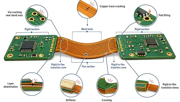
8. Common Flex PCB Failures and Detection Methods
Flex PCB failures typically originate from mechanical stress interacting with electrical structures. Understanding failure signatures allows engineers to select appropriate testing strategies.
| Failure Mode | Root Cause | Detection Method |
|---|---|---|
| Cracked traces | Repeated bending fatigue | Bend or flex-cycle testing |
| Intermittent continuity | Micro-fractures under motion | Dynamic electrical testing |
| Delamination | Adhesion degradation | Peel strength & cross-section analysis |
| Corrosion | Moisture or contamination | Insulation resistance testing |
| Impedance instability | Geometry variation | TDR measurement |
| Short circuits | Debris or deformation | Isolation testing |
This correlation between failure mechanisms and testing methods enables targeted reliability improvement rather than generalized inspection.
Closing Perspective
As flex PCBs continue enabling thinner, lighter, and more mechanically adaptive electronics, validation strategies must evolve accordingly.
Testing under real mechanical conditions, combined with system-level functional verification and advanced inspection techniques, transforms electrical testing from a manufacturing checkpoint into a predictive reliability framework.
For modern electronics engineers, mastering these validation methods is essential to delivering products that succeed not only in the lab—but throughout their operational lifetime.
9. Design for Testability (DFT) in Flex PCBs
Electrical testing efficiency is strongly influenced by decisions made during the design phase.
Many testing challenges associated with flex PCBs originate not from testing limitations but from insufficient consideration of Design for Testability (DFT) principles during layout development.
Unlike rigid boards, flex circuits often have irregular geometries, limited rigid support, and constrained routing areas.
These characteristics make probe access difficult and increase testing complexity if validation requirements are not planned early.
Adding dedicated test points remains one of the most effective DFT strategies.
Properly spaced pads or edge connectors allow reliable electrical contact without mechanically stressing the flexible substrate.
Engineers must balance routing density against accessibility, particularly in fan-out regions where probing space is limited.
Probe accessibility directly affects test yield and cost. Poor access forces reliance on manual probing or complex fixtures, increasing validation time and introducing operator variability.
Designing uniform probe locations and maintaining consistent pad geometry improves automated testing reliability.
The relationship between DFT decisions and testing efficiency is illustrated below.
| DFT Design Choice | Testing Impact | Result |
|---|---|---|
| Dedicated test pads | Stable probe contact | Higher measurement accuracy |
| Edge connectors | Fast functional validation | Reduced setup time |
| Uniform pad spacing | Automated probing | Improved throughput |
| Early validation planning | Simplified fixtures | Lower testing cost |
Well-implemented DFT reduces debugging effort, shortens production ramp-up, and enables scalable validation as product volumes increase.
10. IPC Standards for Flex PCB Testing
Industry standards provide a common framework for evaluating flex PCB performance and ensuring consistent quality expectations between designers, manufacturers, and OEMs. Compliance with IPC standards significantly improves product credibility and reliability assurance.
Several IPC documents are particularly relevant to flex PCB testing and validation.
| Standard | Scope | Engineering Significance |
|---|---|---|
| IPC-6013 | Qualification and performance specification for flexible PCBs | Defines acceptance criteria and reliability classes |
| IPC-2223 | Design standard for flexible circuits | Guides stack-up, bend areas, and layout practices |
| IPC-TM-650 | Test methods manual | Specifies standardized electrical and environmental tests |
| IPC-9257 | Electrical test guideline | Defines verification procedures for PCB connectivity |
IPC-6013 establishes performance requirements across different reliability classes, from consumer electronics to high-reliability aerospace applications.
IPC-2223 provides design recommendations that directly influence mechanical durability and electrical stability.
IPC-TM-650 standardizes testing methodologies, ensuring repeatable measurement conditions across manufacturers.
IPC-9257 focuses on electrical verification processes, helping engineers validate net integrity and isolation performance.
Adhering to these standards strengthens supplier qualification processes and builds trust across the electronics supply chain.
11. Best Practices to Improve Flex PCB Reliability
Flex PCB reliability is determined by the interaction between material selection, mechanical design, and validation strategy.
Experience across multiple industries shows that several engineering practices consistently reduce failure risk.
Mechanical stress management remains the most influential factor. Maintaining a bend radius of at least ten times the circuit thickness significantly lowers copper strain and prolongs fatigue life.
Designs operating below this threshold frequently experience premature conductor cracking.
Material selection also plays a decisive role. Polyimide substrates dominate high-reliability flex applications due to their thermal stability, mechanical endurance, and low dielectric variation compared with polyester alternatives.
Trace orientation relative to bending direction further affects durability. Routing conductors perpendicular to the bend axis distributes strain more evenly and minimizes elongation stress along copper traces.
Reliability outcomes improve substantially when electrical and mechanical testing are performed together rather than independently.
| Design Practice | Reliability Benefit |
|---|---|
| Bend radius ≥10× thickness | Reduced copper fatigue |
| Polyimide substrate | Improved thermal and mechanical stability |
| Perpendicular trace routing | Lower strain concentration |
| Combined mech-electrical testing | Early failure detection |
These practices convert reliability from reactive troubleshooting into proactive engineering control.
12. Expert Insights: How to Avoid Hidden Failures
Hidden failures represent the most costly category of flex PCB defects because they escape production testing and emerge only during field operation. Preventing them requires a shift in testing philosophy.
Experienced reliability engineers emphasize testing under realistic mechanical conditions. Electrical validation performed only in flat configurations provides incomplete insight into actual performance.
Another critical insight involves measurement interpretation. Traditional pass/fail criteria often miss early degradation signals. Monitoring resistance trends over time allows engineers to detect fatigue progression before catastrophic failure occurs.
Equally important is combining functional and electrical testing. A circuit may meet electrical specifications yet fail at the system level due to timing instability, signal distortion, or interface sensitivity.
Early validation during the design phase provides the greatest return on investment. Detecting structural weaknesses before tooling or mass production avoids costly redesign cycles.
| Common Mistake | Recommended Practice |
|---|---|
| Static-only testing | Dynamic mechanical validation |
| Pass/fail evaluation | Trend-based monitoring |
| Isolated electrical tests | Integrated functional testing |
| Late-stage validation | Early design verification |
Organizations that adopt these practices consistently report lower field failure rates and shorter product qualification cycles.
13. Conclusion: Building Reliable Flex PCBs Through Testing and Validation
Flex PCB performance depends on more than accurate fabrication; it relies on comprehensive validation throughout the product lifecycle.
Electrical testing ensures that conductive networks meet design intent, while functional validation confirms that the complete system performs reliably under real operating conditions.
When combined with dynamic mechanical testing, advanced inspection methods, and standards-based verification, testing becomes a predictive tool rather than a reactive quality check.
This integrated approach enables engineers to identify latent defects early, reduce warranty risks, and deliver products capable of long-term operation in demanding environments.
As electronic systems continue to evolve toward thinner, lighter, and more mechanically adaptive designs, robust testing and validation strategies will remain the foundation of flex PCB reliability.

