
High-Shielding FPCB: A Practical Guide to Materials, dB Ratings and Selection
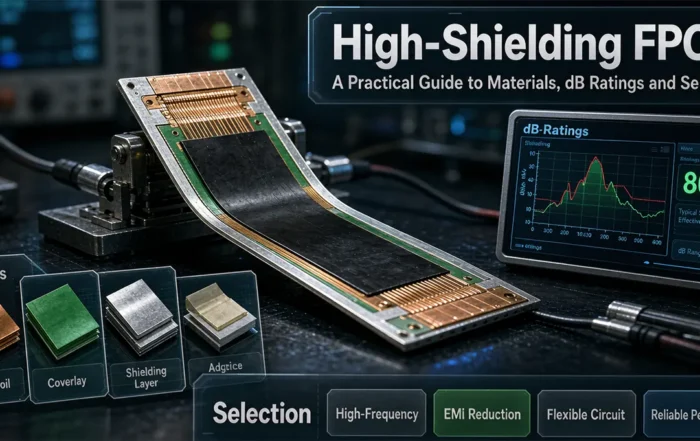
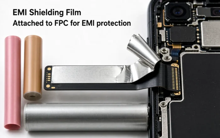
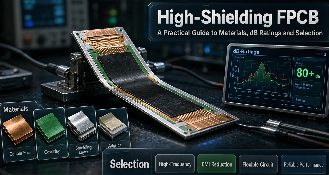
A High-Shielding FPCB is a flexible circuit with a dedicated shielding layer — bonded film, printed silver ink, or plated copper — that typically delivers 60–80 dB attenuation from 100 MHz to 10 GHz. It protects sensitive nets and nearby antennas while keeping the board thin, light, and bendable.
What “High-Shielding” Really Means in dB Terms
Not every flex with a metal layer qualifies as high-shielding. In practice, the label should mean 60 dB or better across the band that matters to your design.
Therefore, ask three questions before you compare supplier numbers: which test method, which frequency, and which specimen? Common references are ASTM D4935 for far-field plane-wave attenuation, IEC 62333-2 for thin shielding films, and a microstrip coupon for near-field, on-board behavior.
A film rated 75 dB at 1 GHz may drop to 55 dB at 10 GHz. Always request an attenuation curve, not a single headline figure.
Stack-Up: Where the Shield Sits
A typical high-shielding build, from the outside in:
1. Coverlay (polyimide plus adhesive) for mechanical and chemical protection.
2. Shield layer — laminated film, printed silver, or plated copper.
3. Conductive adhesive or plated via connecting the shield to ground.
4. Ground copper plane on the base polyimide.
5. Base film, adhesive, and signal traces.
The ground plane is the real reference. Without a low-impedance path to it, the shield floats and the attenuation collapses. On an HDI rigid-flex PCB, therefore, wrap only the flex tail and keep the rigid section clear of the film.
Three Ways to Build the Shield
Each EMI Shielding Method trades attenuation against thickness, bend life, and cost. The table below shows typical ranges for volume production.
| Method | Typical attenuation | Added thickness | Dynamic bend | Cost | Rework | Maturity |
|---|---|---|---|---|---|---|
| Plated copper (Cu + Ni) | 60–80 dB | 12–25 µm | Poor to fair | Medium–high | Hard | High |
| Printed silver ink | 40–60 dB | 8–15 µm | Fair | Low–medium | Fair | High |
| Bonded shielding film | 60–80 dB | 20–40 µm | Good | Medium | Fair (peel and re-laminate) | High |
Copper plating gives the best conductivity per micron and carries current well, yet it cracks at tight bend radii. Silver ink is the cheapest and fastest option, but its 40–60 dB window rarely justifies a “high-shielding” claim above 3 GHz. Shielding film, for example, pairs a thin metal layer with conductive adhesive and survives dynamic bending far better than plating.
Shielding Film Lamination: Step by Step
1. Pre-bake the panel at 120–150 °C to remove moisture.
2. Plasma-clean or micro-etch the ground pads; oxide blocks conductivity.
3. Open windows for pads, test points, and components, keeping at least 0.3 mm clearance to the film edge.
4. Laminate with a hot press, typically 160–180 °C, 1–3 MPa, 60–120 s, following the supplier’s cure curve.
5. Cure the adhesive fully; under-cured film creeps and lifts during reflow.
6. Fill or plate the ground vias so the shield bonds to the plane.
7. Inspect by cross-section, peel strength, and a dB coupon cut from the same lot.
Design Checklist Before You Release the Gerbers
- Ground via pitch ≤ 3 mm, or λ/20 at your highest frequency, whichever is tighter.
- Keep openings small; any slot longer than λ/20 leaks.
- Control glue squeeze-out, especially near fine-pitch pads.
- Expect a capacitance shift: the shield loads the trace, so retune differential impedance targets by roughly 3–8 %.
- Plan for heat: the shield reduces FPCB heat dissipation, so add thermal vias or thicker copper under hot components.
- Define the termination early — crimp terminals for FPCB connectors on pluggable tails, or laser welding FPCB for permanent ground straps.
Bend Life, Salt Spray, and Damp Heat
Shielding data from a flat coupon says little about field reliability. Therefore, qualify the shield on the finished flex, not on raw material.
For dynamic flexing, a practical target is 100,000 cycles at a 1.5–2 mm bend radius with less than 3 dB drift. After 500 h at 85 °C/85 % RH, peel strength should stay above 0.8 N/mm. A 48 h salt spray test should show no visible corrosion on the ground pads.
How to Choose: A Short Decision Path
- Above 3 GHz in tight space: bonded shielding film with a silver or copper layer.
- Static bend, cost-driven, moderate attenuation: printed silver ink.
- High current, high reliability, limited flexing: plated copper.
- Antenna keep-out zones: segmented or patterned shield to avoid detuning.
Where High-Shielding FPCB Is Used
Smartphones and wearables use shielding film around camera modules and antenna flexes. Medical catheters and bench instruments favor plated options for repeatable ground. Automotive camera and radar tails often combine shielding with a stiffener.
Because these designs pack many layers into small spaces, teams frequently pair the shield with an HDI rigid-flex PCB inside compact flexible circuit boards.
Fitting the Shield Into Your FPCB Build
Sequence matters. Most shielding films are laminated after coverlay and electrical test, then reflowed together with SMT; a few must be applied after SMT. Confirm reflow compatibility (260 °C, about 10 s, three passes) with your supplier early.
Yield risks cluster at three points: bubbles under the film, wrinkles in bend zones, and adhesive squeeze-out on fine-pitch pads. High-current designs also need a different copper strategy, which is why our High-Shielding FPCB manufacturing guide covers heavy-copper variants.
Key Takeaways
- “High-shielding” should mean ≥60 dB, with a stated method and frequency.
- Film, silver ink, and plating each win in a different design corner.
- Ground vias and a solid reference plane matter more than the shield material itself.
- Test bend, damp heat, and salt spray on the finished flex.
Send your stack-up, target frequency band, and bend radius. Our engineers will return a shielding recommendation and a sample plan within two working days.
Frequently Asked Questions
How much attenuation does a High-Shielding FPCB provide?
Typically 60–80 dB from 100 MHz to 1 GHz for film and plated copper builds, falling to about 50–60 dB near 10 GHz. Ask for a curve labeled with the test method and specimen type.
Shielding film or copper plating — which should I choose?
Choose plating for static, high-current, high-reliability boards where flexing is limited. Choose film for thin profiles, dynamic bending, and easier rework.
Does the shield survive repeated bending?
Yes, if the metal layer is thin and the bend radius stays at 1.5–2 mm or more. Expect under 3 dB drift after 100,000 cycles; plated copper can crack at tight radii.
Does the shielding layer change my impedance?
Yes. It adds capacitance to ground and lowers trace impedance by roughly 3–8 %, so retune trace width or dielectric spacing before release.
When in the build is the shield laminated?
Usually after coverlay and electrical test and before SMT. Confirm reflow compatibility with your film supplier first.
Related Posts
- Crimp Terminals for FPCB Connectors: Experimental Study — Related article
- HDI Rigid-Flex PCB Manufacturing for Medical Electronics — Related article
- EMI Shielding Method for FPC and Flex Circuits: Complete Guide — Related article
- Laser Welding FPCB: Time, Pressure & Temperature Effects — Related article
- AI-Driven Optimization of Flexible Circuit Boards Production — Related article