Unequal-Thickness Rigid-Flex PCB Single-Press Lamination Process
Unequal-Thickness Rigid-Flex PCB Single-Press Lamination Process
In the field of printed circuit boards (PCBs), rigid-flex printed circuit boards (R-FPCBs) are widely used in sectors with extremely high requirements for space utilization and reliability—such as aerospace, military equipment, and high-end electronic devices—due to their unique combination of rigidity and flexibility.
With the rapid advancement of technology, the PCB industry—as the foundational pillar of the electronic information sector—is experiencing vigorous growth.
Against this backdrop of prosperity, market demand for R-FPCBs is steadily increasing due to their exceptional space utilization efficiency and signal transmission stability.
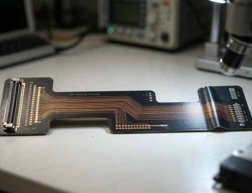
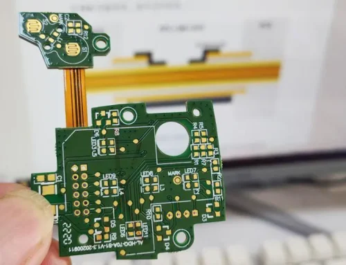
The author’s organization undertook the development of an R-FPCB with a special structure characterized by varying thicknesses in the rigid regions: 2.5 mm for the main board and 2.0 mm for the secondary board, as shown in Figure 1.
When addressing such products, the traditional two-step lamination process has revealed issues such as long processing cycles, high costs, and poor quality consistency, making it difficult to meet market demand.
Therefore, the development of an efficient and precise single-step lamination process is urgently needed.
The goal is to establish a production process that maintains a thickness difference of no more than 0.5 mm between the rigid sections, thereby significantly improving production efficiency and product quality.
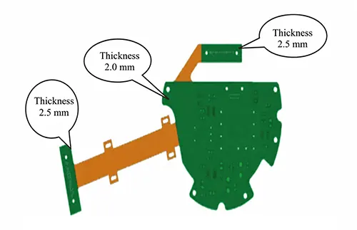
Figure 1. Schematic diagram of a special structure R FPCB product
Process Design
Materials and Equipment
Material Requirements: The substrate material is flexible board SF202 and cover film SF305C; the rigid board material is TU-752. Production quantity: 24 pieces.
Testing Equipment: Metallographic microscope, 2D measuring machine, vector network analyzer.
Process Flow
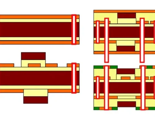
The main process flow is shown in Figure 2.
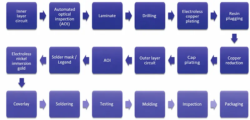
Figure 2 Process Flow
Key Control Points
The processing challenge lies in the fact that a single plate has varying thicknesses.
The process parameters and requirements for the key control points are shown in Table 1.
| Process Step | Requirements | Process Parameters & Methods |
|---|---|---|
| Data Processing | Design step-frame routing data to achieve different board thicknesses in a single lamination. Data accuracy controlled within ±0.01 mm. | Use Computer-Aided Manufacturing (CAM) to design the step-frame routing data. Precisely define the routing boundaries according to a 0.5 mm thickness difference (step-frame design shown in Figure 3). |
| Physical Simulation | Evaluate the stress distribution during lamination and verify the feasibility of prepreg stack-up processing. | Validate the thicknesses of the main board and sub-board through physical simulation to predict the feasibility of the laminated prepreg process. |
| Lamination | Ensure uniform pressure across areas of different thicknesses. No delamination defects are permitted after lamination. | Lamination conditions: Temperature: 200–220°C; Pressure: 25–35 kg/cm²; Time: 2.5–3.5 h.Cushioning pad options:① Use a 1.2 mm high-performance cushioning paper.② Do not use a cushioning paper. |
| Drilling | Reduce hole-entry burrs (<5%); Positioning accuracy: ±0.020 mm; Hole wall roughness: <0.025 mm. | Backing board options:① Use a pressure-sensitive backing board with a special coating.② Do not use a pressure-sensitive backing board.After drilling, perform manual fine polishing using #800 sandpaper and a pneumatic grinder to ensure hole quality. |
| Outer Layer Lamination | Dry film must adhere firmly. No bubbles are allowed in the circuit area. Bubble ratio in non-functional areas should be <5%. | Lamination equipment options:① Use a vacuum laminator.② Use a conventional laminator.Inspect dry-film bubbles using optical inspection equipment. |
| Solder Mask | Provide uniform coating over high- and low-profile surfaces. Thickness uniformity should be ≥80% (minimum/maximum thickness ratio). No exposed copper is permitted on the surface. | Apply the solder mask using advanced low-pressure spray coating equipment, combined with intelligent spray path planning. |
| Coverlay Routing | Routing depth must be properly controlled without scratching the flexible board. | Use CNC programming for precise routing depth control and verify the routing depth with high-precision measuring instruments. |
Table 1. Key Process Control Parameters and Requirements
Processing Procedures and Results
See Table 2 for data on the processing procedures and results. See Table 3 for the product processing results.
| Item | Key Control Point | Process Data | Result |
|---|---|---|---|
| Data Processing | Design step-frame routing data | Data accuracy controlled within ±0.01 mm | Pass |
| Physical Simulation | Feasibility of prepreg stack-up during lamination | Simulation results are highly consistent with actual production and design requirements | Pass |
| Accuracy of prepreg stack-up | Prepreg stack-up accuracy reached 100% | Pass | |
| Lamination | Delamination inspection | ① Using a 1.2 mm high-performance cushioning paper during lamination: No delamination defects found | ① Pass |
| ② Without cushioning paper: 7 delamination defects, accounting for 29% | ② Fail | ||
| Drilling | Hole wall roughness ≤ 0.025 mm | Measured hole wall roughness: 0.01 mm | Pass |
| Burr removal | ① Drilling with a pressure-sensitive backing board: No hole-entry burr defects | ① Pass | |
| ② Drilling without a pressure-sensitive backing board: 15 hole-entry burrs, accounting for 63% | ② Fail | ||
| Outer Layer Circuit | Lamination quality verification. No dry-film bubbles are allowed in the effective circuit area; bubbles in the non-effective area should account for <5% | ① Vacuum laminator used: No dry-film bubble defects in either effective or non-effective circuit areas | ① Pass |
| ② Without a vacuum laminator: 24 dry-film bubbles in the effective circuit area (100%); 16 bubbles in the non-effective area (67%) | ② Fail | ||
| Solder Mask | Spray-coated solder mask ink thickness uniformity ≥ 80% | Minimum ink thickness: 39 μm; Maximum: 45 μm; Thickness uniformity: 87%; No exposed copper defects on the surface | Pass |
| Controlled Depth Routing | Cutting depth control | Cutting depth accurately controlled; no scratches on the flexible board | Pass |
Table 2 Key Process Data and Judgment Results
| Item | Specification | Measured Value | Result |
|---|---|---|---|
| Finished Board Thickness | Main board: 2.5 mmSub-board: 2.0 mmThickness tolerance: ±10% | Main board: 2.46 mmSub-board: 1.95 mm | Pass |
| Finished Board Dimensions | 225.00 mm × 203.00 mmEdge tolerance: ±0.15 mm | 224.97 mm × 202.93 mm | Pass |
| Copper Thickness in Through Holes | ≥35 μm | 38–40 μm | Pass |
| ENIG (Electroless Nickel Immersion Gold) Coating Thickness | Nickel: 3.00–5.00 μmGold: 0.03–0.10 μm | Nickel: 4.20 μmGold: 0.08 μm | Pass |
Table 3. Measurement Data and Evaluation Results
Technical Achievements
(1) Successfully developed a highly efficient and precise single-press process for first-order unequal-thickness R-FPCBs, reducing the processing cycle by 50%—from 30 days to 15 days—which significantly improved production efficiency and product quality while lowering production costs.
(2) A process parameter database was established, comprising six key parameters—including engineering treatment, lamination, and drilling—providing a reliable reference for the production of similar products in the future.
Conclusion
The single-press process for first-order unequal-thickness R-FPCBs developed in this study enables the precise forming of a 2.5 mm/2.0 mm unequal-thickness structure in a single pressing operation, overcoming the cycle time bottleneck associated with traditional two-press processes.
Through the innovative design of stepped frame data, boundary control with a thickness difference of 0.5 mm was achieved.
Combined with pressure equalization technology using a 1.2 mm buffer paper spacer, this solved the problem of pressure loss and delamination during lamination across areas of varying thicknesses.
Measurements show that the thickness tolerances for both the main and secondary plates are controlled within ±10%, meeting the requirements of the GJB 7548A—2021 military standard.
This innovation successfully achieves single-press forming technology for first-order unequal-thickness rigid-flex boards.
Furthermore, this process improves efficiency by 50% compared to the traditional two-press process.