From Materials to Design and Assembly: A Comprehensive Guide to Flexible PCB Technology for Smart Glasses
Smart glasses, such as augmented reality (AR) glasses and smart sunglasses, rely heavily on advanced technology to deliver functionality in a compact, wearable form factor.
At the heart of this innovation are flexible printed circuit boards (PCBs), which provide the necessary adaptability and durability for such cutting-edge devices.
If you want to learn about flexible PCB materials for smart glasses, flexible PCB design rules, or rigid-flex PCB assembly processes, you’ve come to the right place.
This guide delves into the world of FPCs for wearable devices and explores key aspects such as the bend radius of flexible PCBs.
What are Flexible PCBs, and Why are They Essential for Smart Glasses?
Flexible PCBs, commonly referred to as FPCs (Flexible Printed Circuits), are thin, lightweight circuit boards made from flexible materials that can be bent and folded without breaking.
Unlike traditional rigid PCBs, these circuits can conform to unique shapes, making them an ideal choice for the compact and curved designs found in smart glasses.
They save space, reduce weight, and withstand repeated bending cycles, which is why they are the preferred choice for FPCs in wearable devices.
In smart glasses, components must be mounted within slim frames or curved lenses, and flexible PCBs provide the necessary connections for displays, sensors, batteries, and processors.
They enable the seamless integration of technology into form factors that prioritize user comfort and aesthetics.
Without the adaptability of flexible circuits, the stylish designs of modern smart glasses would be nearly impossible to achieve.
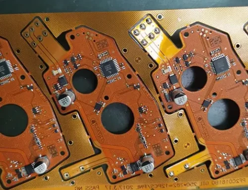
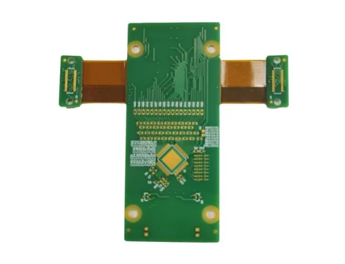
Flexible PCB Materials for Smart Glasses: Choosing the Right Substrate
The performance and reliability of flexible PCBs in smart glasses depend on the materials used.
Selecting the appropriate flexible PCB material for smart glasses requires balancing factors such as flexibility, thermal resistance, and electrical performance.
The following are the primary materials commonly used in these applications:
Polyimide (PI):
Due to its excellent thermal stability (up to 400°C) and mechanical strength, this is the most widely used substrate material for flexible PCBs.
Polyimide can withstand thousands of bending cycles, making it ideal for the dynamic environment of smart glasses.
Polyester (PET):
PET is a more cost-effective option. While it is not as durable as polyimide, it still offers good flexibility for static or low-bending applications.
It is typically used in wearable device designs with less demanding requirements.
Copper Foil:
Copper is the standard conductive material in flexible PCBs. Rolled annealed (RA) copper is preferred over electro-deposited (ED) copper because it offers better flexibility and fatigue resistance, which is critical for the repeated bending of smart glasses.
Adhesives and Cover Layers:
Adhesives bond the layers of the flexible PCB, while cover layers (protective films) shield the circuitry.
These materials must maintain flexibility and adhesion under pressure to prevent delamination during use.
When designing smart glasses, engineers typically prioritize the durability of polyimide-based materials, especially in high-end AR glasses where reliability is critical.
Material selection also impacts signal integrity; polyimide offers low dielectric loss for high-frequency applications such as 5G connectivity in smart devices.

Fig 1
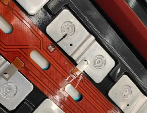
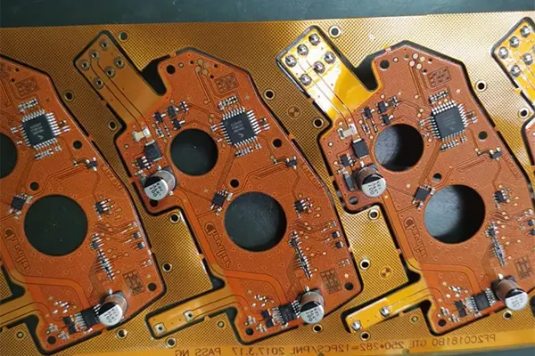
Flexible PCB Design Rules: Essential Guidelines for Smart Glasses
Designing flexible PCBs for smart glasses requires adherence to specific design rules to ensure functionality and longevity.
Poor design can lead to fractures during bending, signal loss, or malfunctions. The following are the basic guidelines to follow:
1. Optimize the Bending Radius
The bending radius of a flexible PCB is a critical parameter. A tighter bending radius increases stress on the circuit, which can cause cracks in the copper traces.
As a general rule, for dynamic bending (repeated bending), the minimum bending radius should be at least 10 times the PCB thickness, and for static bending (one-time installation), the minimum bending radius should be at least 3 times the PCB thickness.
For a 0.1 mm thick flexible PCB, this means a minimum dynamic bending radius of 1 mm.
2. Trace Layout and Spacing
Traces should be perpendicular to the bend line to minimize stress. Avoid placing vias or components in the bending area, as they create weak points.
Maintain sufficient spacing between traces (typically 0.1 mm or greater) to prevent short circuits during bending.
3. Use Teardrop-Shaped Pads
At the junction of traces and pads, use teardrop-shaped pads instead of circular pads.
This design reduces stress concentration and prevents trace cracking, particularly in highly bent areas of smart glasses frames.
4. Stack-up Considerations
For multilayer flexible PCBs, balance the stack-up to avoid uneven stress.
Use a symmetrical layer arrangement to place the neutral axis (the plane that does not bear stress during bending) at the center of the board.
This is particularly important for smart glasses, as the PCB may wrap around curved frame components.
By following these flexible PCB design rules, engineers can create reliable circuits capable of withstanding the unique challenges of wearable technology.
For example, a well-designed FPC in smart glasses can withstand over 100,000 bending cycles without signal degradation, ensuring long-term performance.

Fig 2
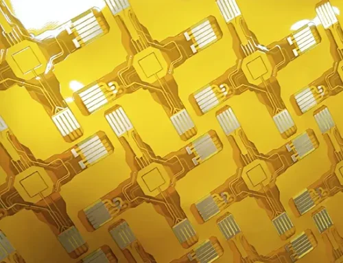
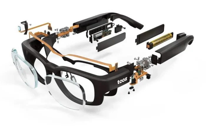
Rigid-Flex PCB Assembly Process: Bridging Flexibility and Stability
Many smart glasses designs incorporate rigid-flex PCBs, which combine a rigid section for component mounting with a flexible section for connectivity.
The rigid-flex PCB assembly process is more complex than that of standard flexible PCBs, but it offers unmatched versatility for compact devices. Here is a step-by-step overview of the process:
Material Preparation:
The process begins with preparing the rigid and flexible materials, typically FR4 for the rigid sections and polyimide for the flexible areas.
These materials are laminated together using specialized adhesives to maintain flexibility in designated areas.
Circuit Patterning:
The copper layer is etched to create circuit patterns on both the rigid and flexible sections.
Precision is key to ensuring alignment between layers, particularly in the high-density designs of smart glasses.
- Drilling
and Plating:
Holes are drilled for via and through-hole components, which are then plated with copper to establish electrical connections.
Care must be taken during this step to avoid damaging the flexible areas.
Lamination and Bonding:
The multiple layers are laminated under heat and pressure.
The flexible sections typically require an additional cover layer for protection, while the rigid sections may include a solder mask.
Component Assembly:
Surface-mount components are placed and soldered onto the rigid sections using automated pick-and-place machines.
The flexible areas are typically left free of components to maintain bendability.
Testing and Inspection:
The assembled rigid-flex PCB undergoes electrical testing and visual inspection to detect defects such as open circuits or misaligned layers.
For smart glasses, testing may include simulated bending cycles to verify durability.
The rigid-flex approach is ideal for smart glasses because it allows processors and sensors to be securely mounted in the rigid area while connecting to the display or battery via the flexible section.
This hybrid design reduces the need for additional connectors, saving space and improving reliability.

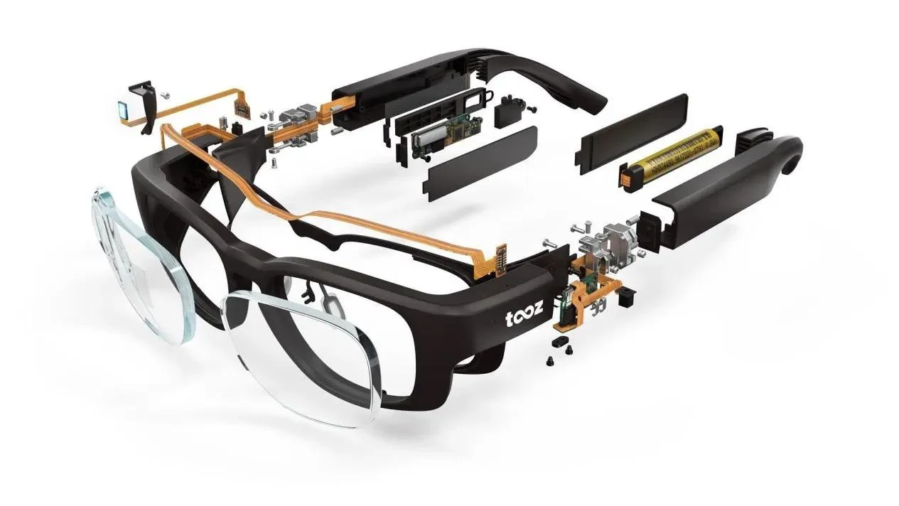
Fig 3 rigid-flex PCB for smart glasses
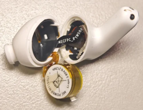
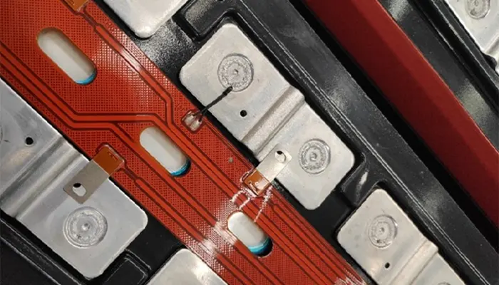
FPCs for Wearable Devices: Advantages for Smart Glasses
Compared to traditional rigid circuits, using FPCs in wearable devices such as smart glasses offers numerous advantages. These advantages directly address the challenges of designing compact, user-friendly technology:
Space Efficiency:
FPCs can be folded or molded to fit into tight spaces, such as the narrow arms of smart glasses, thereby reducing the device’s overall footprint.
Lightweight Design:
FPCs are significantly lighter than rigid PCBs, contributing to the comfort of wearable devices—a key factor for all-day use of smart glasses.
Durability:
High-quality FPCs can withstand repeated bending without failure, ensuring that smart glasses remain functional even after extensive use.
Reduced Interconnects:
By eliminating the need for bulky connectors and cables, FPCs simplify assembly and improve reliability, which is critical for maintaining signal integrity in high-frequency applications.
For example, in AR glasses, FPCs can connect the micro-display in the lens area to the control unit within the frame, bending around corners without adding bulk.
This seamless integration is why FPCs have become a cornerstone of modern wearable technology.

Fig 4 Smart glasses
Challenges and Solutions in the Manufacturing of Flexible PCBs for Smart Glasses
The manufacturing of flexible PCBs for smart glasses presents unique challenges, but technological advancements have provided effective solutions:
Challenge 1: Maintaining Signal Integrity
High-frequency signals in smart glasses (such as wireless connection signals) may degrade due to the thin dielectric layers in flexible PCBs.
To address this, manufacturers use low-loss materials such as modified polyimide and ensure precise impedance control, targeting an equivalent impedance of 50 ohms for optimal performance.
Challenge 2: Ensuring Flexural Durability
Repeated bending can cause fatigue in copper traces. Solutions include using rolled-annealed copper and reinforcing bending areas with stiffeners or additional cover layers to distribute stress evenly.
Challenge 3: Miniaturization
Smart glasses require extremely small PCBs with high-density interconnects. Advanced manufacturing techniques, such as micro-hole laser drilling (with diameters as small as 0.05 mm), enable the creation of compact, high-performance circuits.
By addressing these challenges, manufacturers can produce flexible PCBs that meet the stringent requirements of smart glasses, ranging from durability to signal speed.
Driving the Future of Smart Glasses with Flexible PCBs
Flexible PCBs are the backbone of smart glasses, enabling the stylish, lightweight, and functional designs that users demand.
From selecting the right flexible PCB materials for smart glasses to adhering to flexible PCB design rules and mastering the assembly process for rigid-flex PCBs, every step is critical to success.
Conclusion
Flexible printed circuits play a central role in enabling the compact structure, mechanical resilience, and high functionality required in modern smart glasses.
By combining advanced materials such as polyimide substrates and rolled annealed copper with carefully engineered design rules, FPCs ensure reliable electrical performance under continuous bending and tight spatial constraints.
Proper material selection, optimized bending radius control, and well-structured trace layout directly influence the durability and signal integrity of wearable devices.
At the same time, rigid-flex PCB architectures further enhance system integration by combining mechanical stability with flexible interconnectivity, reducing space requirements and improving overall reliability.
Despite challenges such as signal degradation, mechanical fatigue, and extreme miniaturization, advances in manufacturing processes and material engineering continue to push the limits of what flexible circuits can achieve.
Ultimately, flexible PCBs serve as the foundational technology that makes lightweight, ergonomic, and high-performance smart glasses possible, driving continued innovation in the wearable electronics industry.