Preventing FPCB Pad Cracking: Bump Design, Material Selection & Stamping Guide
Direct answer: FPCB pad bump cracking is most effectively prevented by combining three controls:
- Design— lower bump height, rounded transition profiles, and fillets at pad-to-trace junctions.
- Material — high-ductility copper foil, typically rolled annealed copper, with well-adhered plating.
- Stamping process — progressive forming, proper die clearance, controlled speed/pressure, and adequate pad support.
Avoiding sharp geometric transitions and excessive single-step deformation reduces stress concentration and microcrack initiation. Where application flexing cannot be eliminated, pair these controls with bend and thermal-cycling validation.
Flexible printed circuit boards (FPCBs) provide flexible connections in electronic devices. Bump technology is applied to FPCB connection pads for applications such as SIM card slots in point-of-sale (POS) systems, printer cartridges, and similar devices that require reliable contact and mechanical fastening. Bump reliability directly affects product performance and service life, and bump cracking is a common failure mode during manufacturing, assembly, or use.
1. What Is an FPCB Bump and Why Does Cracking Occur?

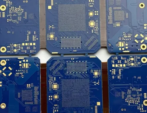
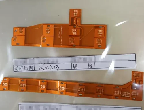
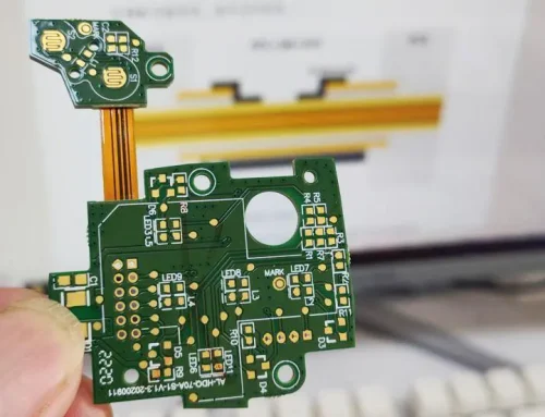
Figure 1: Actual view of the connection pad bumps on an FPCB
Flexible printed circuit boards (FPCBs) are core components used to achieve flexible connections in electronic devices.
To ensure better contact between certain specialized devices and other components, the bump process is employed on the connection pads of FPCBs.
For example, this technology is used in the SIM card slots of point-of-sale (POS) systems, printer cartridges, and other devices.
The reliability of the bumps directly affects product performance and service life, and bump cracking is a common failure mode in FPCBs during manufacturing, assembly, or use.
Cracking typically appears after forming or during repeated mechanical or thermal stress. It is not a single-cause failure; it results from interaction among geometry, material behavior, and process conditions.
Common Crack Initiation Sites
- **Bump-to-pad transition zone:** The base of the bump where the material changes slope is the highest stress concentration area.
- **Grain boundaries:** If the copper foil work-hardens during forming, cracks can propagate along grain boundaries.
- **Plating interface:** Poor adhesion or internal stress in plating layers can initiate peeling or microcracks.
- **Pad-to-trace junction:** Where the pad connects to the trace, especially if the transition is abrupt.
Root Causes Overview
- Abrupt bump geometry with sharp corners or vertical sidewalls.
- Low-ductility copper foil or brittle plating.
- Excessive stamping force, insufficient die clearance, or forming in a single aggressive step.
- Bumps placed too close to bend zones, fold lines, or board edges.
- Repeated flexing or thermal expansion mismatch during end use.
2. Bump Design Rules to Prevent Pad Cracking
Introduction to Bumps
FPCB bump technology refers to the formation of metal bumps with specific heights and shapes at specific locations on an FPCB, as shown in Figure 1.
These protrusions play a critical role in electronic devices by providing electrical connections and mechanical fastening.
Typically, the center of the connection pad is raised through stamping or localized plating to increase its thickness; this paper focuses primarily on the application of stamping methods.
Design Requirements for Pad Connectors
Design the bump with a lower height-to-diameter ratio when the application allows. A shallow dome or rounded trapezoid is generally more crack-resistant than a tall, sharp-edged bump.
- Use a gradual slope transition rather than a steep or vertical wall.
- Increase the fillet radius at the base of the bump to distribute stress over a wider area.
- Keep the bump centered on the pad and away from pad edges where support is lower.
To prevent tearing or collapse of the copper foil during the stamping process, the relationship between the pad height (H), substrate thickness (T), and pad diameter (D) is shown in Figure 2. The specific requirements are as follows:
(1) When the pad height H is greater than 0.5 times the substrate thickness T, the pad diameter must satisfy D ≥ 1.8H. For example, if H = 0.30 mm, then D ≥ 0.54 mm.
(2) When the pad height H = T, the diameter must satisfy D ≥ 2.5H. For example, if T = 0.10 mm, then D ≥ 0.25 mm.

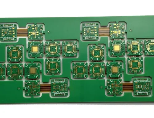
Figure 2: Bump connectors on an FPCB
Pad and Trace Transition Design
- Add a teardrop or fillet at the pad-to-trace junction to reduce notch stress.
- Avoid placing bumps directly over plated through-holes or vias unless the design supports the forming area.
- Do not position bumps on a flex region that will undergo repeated bending unless full dynamic-flex validation is performed.
3. Effect of Connection Pad Design on Bump Cracking
Connection Pad Dimension Specifications
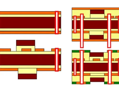
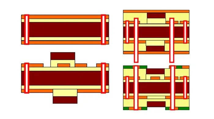
There are two categories of pad sizing constraints: one is defined by the copper foil, known as a copper-defined pad (CD Pad) or non-solder-mask-defined pad (NSMDP), commonly referred to as an “unmasked pad” in FPCB design, as shown in Figure 3(a).
The other type of connection pad is defined by the solder mask pattern, known as a solder mask defined pad (SMDP), commonly referred to as a “masked pad” design in FPCB, as shown in Figure 3(b).
Since FPCBs use a cover film instead of a solder mask, this type of connection pad can be further classified into cover film defined pads and non-cover film defined pads.

Figure 3: Dimensions of the Coupling Plate
Bump Pad Design
Single-Sided Bump Pad Design
Single-sided pad-on-pad designs must be configured as “press-to-pad” types, utilizing a specialized structural design for surface-mount devices (SMD).
This design ensures that the cover film fully presses against the area surrounding the pad, creating a secure bond.
The primary objective is to prevent cracking or damage to the polyimide (PI) substrate during the pad-forming process, as shown in Figure 4.
The PI thickness of FPCB substrates is typically only 25 μm. If the area around the connection pad is not effectively bonded by the cover film, the PI material in that region lacks support.
As a result, it becomes exceptionally fragile. It is highly susceptible to cracking when subjected to mechanical stresses such as stamping, which in turn affects the product’s reliability and service life.

Figure 4: Single-sided FPCB connector board design
Design of Double-Sided Pad Connectors
The pad surface of the double-sided connector features a circular cutout, while the recessed surface is designed as a square, as shown in Figure 5.
It is important to note that the dimensions of the two connector surfaces and their cutouts must differ; if designed with identical dimensions, the connector may detach.
This conclusion has been verified by JaliChuang FPCB.

Figure 5: Design of a Double-Sided FPCB Connector Plate
Pressure PAD Test Protocol and Results
To verify the impact of different pressure PAD designs on pad cracking, conducted an in-depth study on pad surfaces using both pressure PAD and non-pressure PAD designs.
The tests utilized 0.11 mm thick boards made of 12 μm adhesive-free electrolytic copper, with 16 pieces of each design, all stamped using the same set of steel dies.
The results showed that 3 pads (15%) cracked in the pressed PAD design, while 17 pads (85%) cracked in the unpressed PAD design. The test samples are shown in Figure 6.
The experimental results show that cracks appeared in both the pressure-applied PAD and the non-pressure-applied PAD.
However, the pressure-applied PAD design exhibited significantly fewer cracks than the non-pressure-applied PAD, and the severity of the cracks was relatively milder.

Figure 6: Effect of Pressing the PAD vs. Not Pressing the PAD on the Contact Points
4. Material Selection for Crack-Resistant Bumps
Copper Foil Type
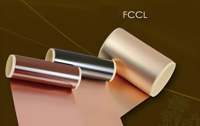
Rolled annealed (RA) copper generally offers higher ductility and better performance in dynamic flex and bump-forming applications than electro-deposited (ED) copper. RA copper has an elongated grain structure that tolerates more deformation before cracking.
- Select RA copper when bump height, forming depth, or flex life is a primary concern.
- Use thinner copper only if electrical and mechanical requirements allow; thinner foil reduces forming force but may reduce overall pad strength.
- Verify copper elongation, tensile strength, and grain structure for the specific foil grade before finalizing the design.
Plating and Surface Finish
Plating layers such as nickel/gold, tin, or solder coatings must have good adhesion and manageable internal stress.
- Avoid excessive nickel thickness if brittleness becomes a risk; nickel can crack and propagate into the copper beneath.
- Specify plating that matches the end-use contact requirements without adding unnecessary stiffness or stress.
- Perform adhesion testing on plated bumps after thermal cycling to identify interface weaknesses.
For a deeper comparison of copper foil types, see RA vs. ED Copper for Flexible PCBs.
Tips: Recommend rolled copper, as electrolytic copper poses a certain risk of bump cracking.
5. Stamping Process Optimization
Identify two main types of dies for stamping protrusions: bakelite dies and steel dies, as shown in Figure 7.

Figure 7: Bakelite jig and steel mold (actual items)
Bakelite molds are inexpensive to manufacture and are suitable for low-cost or single-use applications. Steel molds are more expensive to produce.
However, they offer better cost efficiency in mass production due to the ability to spread costs over a larger volume.
See Table 1 for a detailed comparison of their specific characteristics.
| Comparison Aspect | PCB Fixture (Phenolic / FR-4 Type) | Steel Mold |
|---|---|---|
| Main Material | Phenolic resin base with wood powder filler, compression molded | Steel (e.g., carbon steel, tool steel) |
| Hardness | Lower hardness (Rockwell ~70–90), moderate wear resistance | Higher hardness (Rockwell ~85–98+), strong wear resistance |
| Heat Resistance | Withstands ~120–150°C; may deform or soften under prolonged heat | Excellent heat resistance (some steels withstand >300°C) |
| Electrical Property | Good insulation, suitable for electronics fixtures | Conductive, no insulation |
| Weight | Lightweight, easy to handle and install | Heavy, typically used with stamping presses |
Table 1: Differences Between PCB Fixtures and Steel Molds
Test Protocol and Results for Molds of Different Materials
The test used 0.11mm thick, 12 μm adhesive-free rolled copper sheets.
All test samples featured a PAD design, with 16 pieces per group, and used both bakelite molds and steel molds for stamping.
During the validation process, used both bakelite molds and steel molds to stamp 20 copper-clad laminate PAD bumps.
The results showed that 4 bumps (20%) fractured in the Bakelite molds, and the bump surfaces were sharp and rough.
6. Quality Verification and Failure Analysis
Preventive design and process choices must be verified with targeted inspections and tests.
- **Visual inspection:** Inspect bump edges and pad transitions under magnification for microcracks, necking, or discoloration.
- **Cross-section analysis:** Evaluate the crack path, plating adhesion, and copper grain deformation at the bump base.
- **Thermal cycling:** Expose samples to the expected operating temperature range to reveal fatigue-related cracking.
- **Bend or flex testing:** For FPCBs that will experience dynamic bending, perform repeated bend tests with forming-side orientation matched to the final assembly.
- **Adhesion testing:** Verify plating-to-copper and copper-to-polyimide adhesion after environmental stress.
Documenting these results creates a baseline for comparing future material or process changes.
7. Frequently Asked Questions
**Q: What is the main cause of FPCB bump cracking?**
A: The main cause is stress concentration at the transition between the raised bump and the flat pad. This is aggravated by low-ductility copper, sharp bump geometry, or aggressive single-step stamping.
**Q: Which copper foil is better for preventing bump cracking?**
A: Rolled annealed copper is generally preferred because it offers higher elongation and better resistance to deformation-related cracking than electro-deposited copper. However, the final result also depends on bump design, plating, and stamping parameters.
**Q: Can bump cracking be completely eliminated?**
A: It can be minimized but not always completely eliminated, especially in applications with repeated flexing or thermal cycling. The practical goal is to move the crack initiation threshold beyond the expected product lifetime through design, material, process, and validation controls.
**Q: How does the stamping method affect bump cracking?**
A: Stamping with excessive force, improper die clearance, or a single-step deep form can create microcracks and stress concentrations. Progressive forming with controlled speed, pressure, and pad support reduces cracking risk.
**Q: Where should bump placement be avoided on an FPCB?**
A: Avoid placing bumps directly in dynamic flex zones, fold lines, or too close to pad edges. Bumps in these locations experience higher mechanical stress and are more likely to crack during assembly or use.