Flexible PCB SMT Process: Complete Guide to Flexible Printed Circuit Assembly and Manufacturing
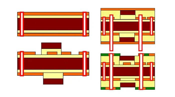
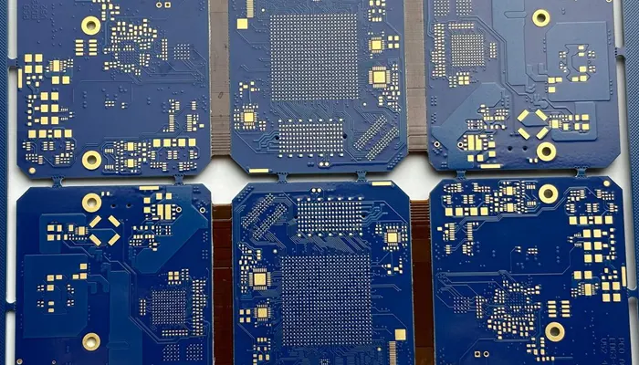
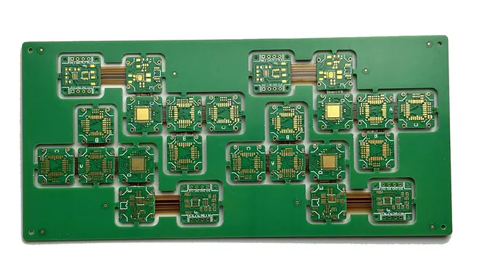
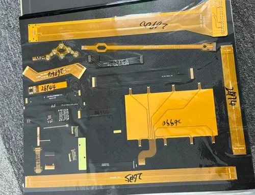
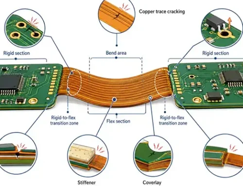
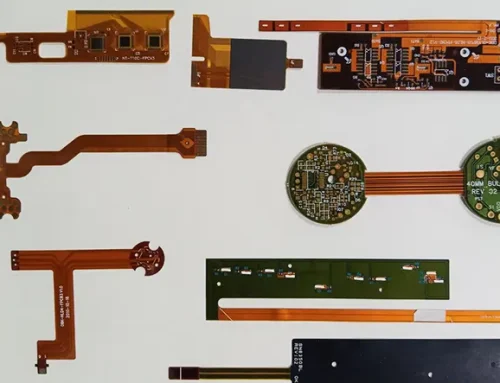
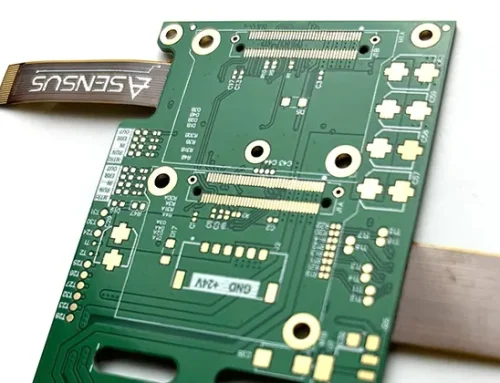
Flexible PCB is a flexible circuit board, also known as a flexible circuit or bendable circuit board, and commonly referred to as a “flex board.”
It is a highly reliable, flexible printed circuit made using polyimide or polyester film as the substrate.
The miniaturization of electronic products is an inevitable trend. Due to space constraints during assembly, a significant portion of surface-mount components (SMDs) in consumer products are mounted on Flexible PCBs to complete the assembly of the entire device.
Flexible PCBs are widely used in digital products, such as calculators, mobile phones, digital cameras, and digital camcorders.
The surface-mount assembly of SMDs on Flexible PCBs has become one of the trends in SMT technology.
According to the definition in JIS C5017, single-sided and double-sided printed circuit boards are single-sided flexible printed circuit boards formed by laminating copper foil onto a PET or PI substrate to create a single-sided circuit, or double-sided flexible printed circuit boards formed by creating circuits on both sides of a PI substrate.
Flexible PCBs are primarily used in the following fields: MP3 and MP4 players, portable CD players, home VCD and DVD players, digital cameras, mobile phones and phone batteries, digital walkie-talkies, as well as in the medical, automotive, aerospace, and military sectors.
Features of Flexible PCB
| Advantages | Disadvantages |
|---|---|
| Lightweight, compact, and thin | Long manufacturing process, high process and environmental requirements, high cost |
| Flexible; can bend, fold, and move freely in three-dimensional space | High scrap rate |
| Greater design flexibility; supports three-dimensional routing | Low mechanical strength |
| Excellent heat dissipation | Inspection is more difficult than for rigid PCBs |
| Higher wiring density | Requires production fixtures; places high demands on fixture design capabilities of engineers |
SMT Production Methods for Flexible PCBs
The process requirements for surface-mount technology (SMT) on Flexible PCBs differ significantly from those of traditional rigid PCB SMT solutions.
To successfully execute the SMT process for Flexible PCBs, proper positioning is of the utmost importance.
Because Flexible PCBs lack sufficient rigidity and are relatively flexible, it is impossible to secure and transport them—and thus to complete basic SMT processes such as printing, component placement, and reflow soldering—without using a specialized carrier board.
The following sections detail the key process requirements for Flexible PCB SMT production, covering pre-treatment, clamping, printing, component placement, reflow soldering, testing, inspection, and panel separation.
RTR Continuous Tape-and-Reel
Roll-to-roll or reel-to-reel, abbreviated as RTR. During the 1980s, a handful of large Flexible PCB manufacturers around the world began establishing RTR production lines.
However, because the process technology used at that time was not yet mature, the yield rate of Flexible PCBs produced on RTR lines was very low.
the late 1990s, driven by the expansion of the TAB and COF markets and the initial maturation of RTR technology, the advantages of this continuous Flexible PCB production equipment and process began to gradually emerge in the manufacture of TAB and COF Flexible PCBs.
By the early 21st century, the technology for producing Flexible PCBs using the RTR method had reached a relatively mature stage.
Schematic Diagram of a REEL-TO-REEL Production Line:
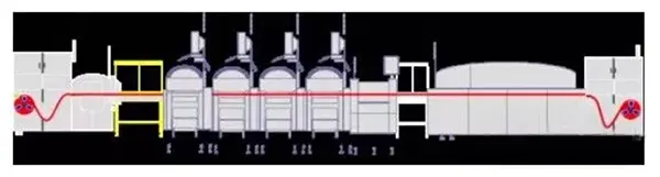
Fig 1: REEL-TO-REEL Production Line
1. Advantages of Reel-to-Reel
- Eliminates the need for operators to perform tasks such as mounting Flexible PCBs onto fixtures.
- Prevents creases and scratches on the Flexible PCB.
- For products requiring a high-cleanroom environment in subsequent processes, such as FOG or NCP, this method avoids contamination from personnel and the environment.
- Simplifies packaging, transportation, and operating conditions.
- Meets the process requirements—such as COF—for ultra-thin, high-end Flexible PCBs.
2. Disadvantages of Reel-to-Reel
- Production line equipment is highly specialized, resulting in a narrow range of applicable products.
- RTR production equipment requires a high initial investment.
- Suitable for ultra-high-volume Flexible PCB production. Not suitable for small-batch, high-variety production models.
Fixture-Mounted Method
This production method focuses on the mounting and securing of Flexible PCBs. The purpose of mounting the Flexible PCB is to use fixtures to transform the Flexible PCB into a “PCB,” allowing the Flexible PCB to undergo SMT just like a “PCB.”
Compared to reel-to-reel, the jig-based placement method is cost-effective, simple, and easy to use; therefore, using jigs for Flexible PCB SMT is currently the most common method in the industry.
This article will discuss the production process based on the jig-based placement method.
Key Process Points for Fixture Attachment Methods
Based on the PCB’s CAD files, the hole positioning data for the Flexible PCB is extracted to manufacture high-precision Flexible PCB positioning jigs and specialized carrier boards, ensuring that the diameters of the positioning pins on the jig match the diameters of the positioning holes on both the carrier board and the Flexible PCB.
Many Flexible PCBs are not uniform in thickness due to the need to protect certain circuit sections or for design reasons; some areas are thicker while others are thinner, and some even incorporate reinforcing metal plates.
Therefore, the interface between the carrier board and the Flexible PCB must be machined, polished, and grooved according to the actual conditions to ensure the Flexible PCB lies flat during printing and assembly.
The carrier board material must be lightweight, thin, high-strength, have low heat absorption, and provide rapid heat dissipation, while exhibiting minimal warping or deformation after repeated thermal shocks.
Commonly used carrier board materials include composite stone, aluminum sheet, silicone sheet, and special high-temperature-resistant magnetized steel sheets.
1. Standard Substrates
Standard substrates are easy to design and quick to prototyped. Common materials for standard substrates include engineering plastics (composite stone) and aluminum sheets.
Engineering plastic substrates have a lifespan of 3,000–7,000 cycles, are easy to handle, offer good stability, do not absorb heat easily, and do not get hot to the touch; however, they cost more than five times as much as aluminum sheets.
2. Aluminum Substrates
They absorb and dissipate heat quickly, with no temperature difference between the interior and exterior. Deformation can be easily repaired.
They are inexpensive and have a long service life. The main drawback is that they become hot to the touch, requiring heat-resistant gloves for handling.
3. Silicone Sheets
This material is self-adhesive, allowing Flexible PCBs to be attached directly without the need for tape.
They are also easy to remove without leaving adhesive residue and are heat-resistant. However, silicone sheets rely on a chemical process; over time, the silicone material ages and loses adhesion.
Additionally, adhesion decreases if the sheet is not cleaned during use. Consequently, they have a relatively short lifespan of 1,000–2,000 cycles at most and are relatively expensive.
4. Magnetic Fixtures
Special high-temperature-resistant (350°C) steel plates undergo a magnetic enhancement treatment to ensure “permanent magnetism” during the reflow soldering process. They offer good elasticity, excellent flatness, and resistance to deformation at high temperatures.
Because the magnetically enhanced steel plates firmly press and flatten the Flexible PCB surface, they prevent the Flexible PCB from being blown up by the reflow air during soldering—thereby avoiding soldering defects, ensuring stable soldering quality, and improving yield rates.
Provided there is no intentional damage or accidental breakage, these fixtures can be used indefinitely and have a long service life. Magnetic fixtures also provide thermal insulation for the Flexible PCB, ensuring no damage occurs to the Flexible PCB when the board is removed.
However, magnetic fixtures have a complex design and a high unit cost, making them cost-effective only for high-volume production.
Pre-baking
Flexible PCB materials are prone to moisture absorption. When a moisture-contaminated Flexible PCB undergoes high-temperature soldering, it may develop bubbles and delamination, resulting in scrap.
Therefore, Flexible PCB suppliers are typically required to vacuum-pack the materials upon delivery. However, vacuum packaging is not foolproof, so it is best to pre-bake the Flexible PCB before surface-mount assembly.
The pre-baking parameters—including temperature, baking time, and stack height—must be determined by comprehensively considering the Flexible PCB material, thickness, oven type, and baking trays, and should be finalized only after engineering testing.
After baking, the Flexible PCB must be cooled to room temperature before being used in production; otherwise, the hot Flexible PCB may cause thermal collapse of the solder paste.
Two additional factors need to be monitored here: cooling time and the time required for re-baking after exceeding the shelf life—both of which must be determined through engineering testing.
Solder Paste Printing for Flexible PCBs
Flexible PCBs do not have any special requirements regarding the composition of solder paste; factors such as solder ball size and metal content depend on whether the Flexible PCB contains fine-pitch ICs.
However, Flexible PCBs have high requirements for solder paste printability.
The solder paste should possess excellent thixotropy, be easy to print and release from the stencil, and adhere firmly to the Flexible PCB surface without defects such as poor release, stencil aperture blockage, or sagging after printing.
Because Flexible PCBs are mounted on carrier boards and secured with high-temperature-resistant tape for positioning, their surfaces are not perfectly flat.
Consequently, the printing surface of an Flexible PCB cannot be as flat or have the uniform thickness and hardness of a PCB.
Therefore, metal squeegees should not be used; instead, polyurethane squeegees with a hardness of 80–90 degrees should be employed.
The solder paste printer should ideally be equipped with an optical positioning system; otherwise, print quality will be significantly affected.
Although the Flexible PCB is secured to the carrier board, there will always be a slight gap between the Flexible PCB and the carrier board—this is the key difference from rigid PCBs.
Consequently, the settings of the equipment parameters will also have a significant impact on the printing results.
The printing station is also a critical area for preventing contamination of the Flexible PCB.
Operators must wear finger cots while working and keep the workstation clean, frequently wiping the stencil to prevent solder paste from contaminating the Flexible PCB’s gold fingers and gold-plated buttons.
Solder Paste Printing for Flexible PCBs
Flexible PCBs do not have any special requirements regarding the composition of solder paste; factors such as solder ball size and metal content depend on whether the Flexible PCB contains fine-pitch ICs. However, Flexible PCBs have high requirements for solder paste printability.
The solder paste should possess excellent thixotropy, be easy to print and release from the stencil, and adhere firmly to the Flexible PCB surface without defects such as poor release, stencil aperture blockage, or sagging after printing.
Because Flexible PCBs are mounted on carrier boards and secured with high-temperature-resistant tape for positioning, their surfaces are not perfectly flat.
Consequently, the printing surface of an Flexible PCB cannot be as flat or have the uniform thickness and hardness of a PCB.
Therefore, metal squeegees should not be used; instead, polyurethane squeegees with a hardness of 80–90 degrees should be employed.
The solder paste printer should ideally be equipped with an optical positioning system; otherwise, print quality will be significantly affected.
Although the Flexible PCB is secured to the carrier board, there will always be a slight gap between the Flexible PCB and the carrier board—this is the key difference from rigid PCBs.
Consequently, the settings of the equipment parameters will also have a significant impact on the printing results.
The printing station is also a critical area for preventing contamination of the Flexible PCB.
Operators must wear finger cots while working and keep the workstation clean, frequently wiping the stencil to prevent solder paste from contaminating the Flexible PCB’s gold fingers and gold-plated buttons.
Flexible PCB Assembly
Once an Flexible PCB is mounted onto a fixture, it effectively becomes a “PCB,” and the issue of Flexible PCB warping is resolved.
At that point, the assembly process becomes very straightforward and is not much different from PCB assembly.
However, because Flexible PCBs contain fewer components, they must be assembled in panel form; therefore, the key challenge in Flexible PCB assembly is how to use the placement machine efficiently.
1. When Flexible PCBs are received as panelized boards
SMT placement for panelized Flexible PCBs is relatively simple. In this case, the only consideration is the impact of the defect rate per panel on placement efficiency. It is essential to ensure that the placement machine’s cycle time remains at its maximum even when the defect rate is at its highest.
2. When Flexible PCBs are supplied as single panels
Single-panel Flexible PCBs must first be assembled into panelized assemblies on a fixture before they can enter production.
The number of panelized assemblies directly affects placement efficiency.
Since Flexible PCBs primarily consist of chips, with relatively few ICs and connectors, we recommend that the number of panelized assemblies be a multiple of the number of indexers on each arm of the placement machine.
For example, on a Siemens D4 placement machine, each arm has 12 indexers, so the number of Flexible PCB panels per assembly can be 12 per assembly or a multiple of 12 per assembly.
The advantage of this approach is that each cycle can pick up a full set of components without waste, and it facilitates program optimization (manual fine-tuning after automatic optimization).
When Flexible PCBs are assembled into a 12-panel panel, the position of each Flexible PCB will vary to some extent due to the positioning accuracy of the fixtures and the precision of the Flexible PCB positioning holes.
Therefore, during SMT placement, each Flexible PCB must be identified using MARK points; for example, a 12-panel assembly requires the identification of 24 MARK points, resulting in a significant loss of efficiency.
We recommend a solder paste mark point technology, as shown in the figure below.
Using this technology not only reduces the number of mark points to just two but also significantly improves quality issues such as component standing upright and cold solder joints.
However, before using solder paste mark points, you must confirm whether the placement machine’s camera is equipped with a blue light and a 45-degree light source; otherwise, the camera will need to be modified by adding a 45-degree blue light source.
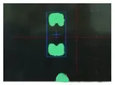
Fig 2: Solder paste mark point technology
Reflow Soldering of Flexible PCBs:
A forced-air convection infrared reflow oven should be used, as this ensures a more uniform temperature distribution across the Flexible PCB, thereby reducing the occurrence of soldering defects.
If single-sided tape is used, since it can only secure the four edges of the Flexible PCB, the central portion may deform under the hot air, causing the pads to tilt.
As a result, molten solder (liquid tin at high temperatures) may flow, leading to open joints, short circuits, and solder balls, which in turn increases the process defect rate.
1) Temperature Profile Testing Method:
Due to differences in the heat absorption characteristics of carrier boards and the variety of components on the Flexible PCB, the rate at which they heat up and the amount of heat absorbed during the reflow soldering process vary.
Therefore, carefully setting the reflow oven’s temperature profile has a significant impact on soldering quality.
A reliable method is to place two carrier boards with Flexible PCBs on either side of the test board, based on the actual production spacing between carrier boards.
At the same time, mount components on the Flexible PCB of the test board, solder the test temperature probe to the test points using high-temperature solder wire, and secure the probe leads to the carrier board with high-temperature-resistant tape.
Note that the high-temperature-resistant tape must not cover the test points.
Test points should be selected near the solder joints and QFP pins along the edges of the carrier board; test results obtained this way will more accurately reflect actual conditions.
2) Temperature Curve Settings:
During oven temperature debugging, because Flexible PCBs do not distribute heat evenly, it is best to use a temperature curve consisting of heating, holding, and reflow stages.
This makes it easier to control parameters in each temperature zone and minimizes thermal shock to both the Flexible PCB and components.
Based on experience, it is best to set the oven temperature to the lower limit specified in the solder paste technical requirements.
The airflow speed in the reflow oven should generally be set to the lowest speed the oven can accommodate, and the reflow oven conveyor chain must be stable, with no shaking.
Flexible PCB Inspection, Testing, and Depaneling:
Since the carrier boards absorb heat in the oven—particularly aluminum carrier boards—they emerge at a high temperature.
Therefore, it is best to install forced-air cooling fans at the oven outlet to facilitate rapid cooling.
At the same time, operators must wear heat-resistant gloves to avoid burns from the hot carrier boards.
When removing the soldered Flexible PCBs from the carrier boards, apply even pressure and avoid using excessive force to prevent tearing or creasing of the Flexible PCBs.
The removed Flexible PCBs should be visually inspected under a magnifying glass with at least 5x magnification, focusing on issues such as residual adhesive on the surface, discoloration, solder on gold fingers, solder balls, cold solder joints on IC pins, and short circuits.
Since the surface of an Flexible PCB is unlikely to be perfectly flat—which leads to a high false-positive rate in AOI—Flexible PCBs are generally not suitable for AOI inspection.
However, with the aid of specialized test fixtures, Flexible PCBs can undergo ICT and FCT testing.
Since most Flexible PCBs are supplied on panel form, it may be necessary to separate them before performing ICT or FCT testing.
Although separation can be accomplished using tools such as blades or scissors, this method results in low operational efficiency and quality, as well as a high scrap rate.
For high-volume production of irregularly shaped Flexible PCBs, it is recommended to fabricate a dedicated Flexible PCB die-cutting mold for separation.
This can significantly improve operational efficiency, while ensuring the cut edges of the Flexible PCBs are neat and aesthetically pleasing.
Additionally, the internal stress generated during die-cutting is minimal, effectively preventing solder crack.
Flexible PCBs received as panelized assemblies require separation. Depending on the connection method used in the panel assembly, different separation methods must be selected.
1. Micro-connection Panelization Method
Flexible PCBs that use micro-connections have only a slight connection at the joints with the Flexible PCB panel; the Flexible PCB can be separated from the panel by gently tearing it by hand.
However, the bonding strength of micro-connections is too weak, and the Flexible PCB may accidentally detach from the panel, causing printing misalignment.
Therefore, for Flexible PCBs with high component density and narrow pad spacing, the micro-connection method is not suitable for panelization; instead, the connecting web method should be used.
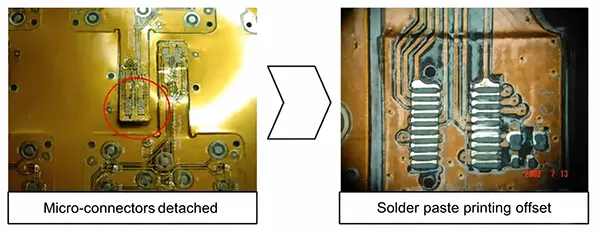
Fig 3: Micro-connection Panelization Method
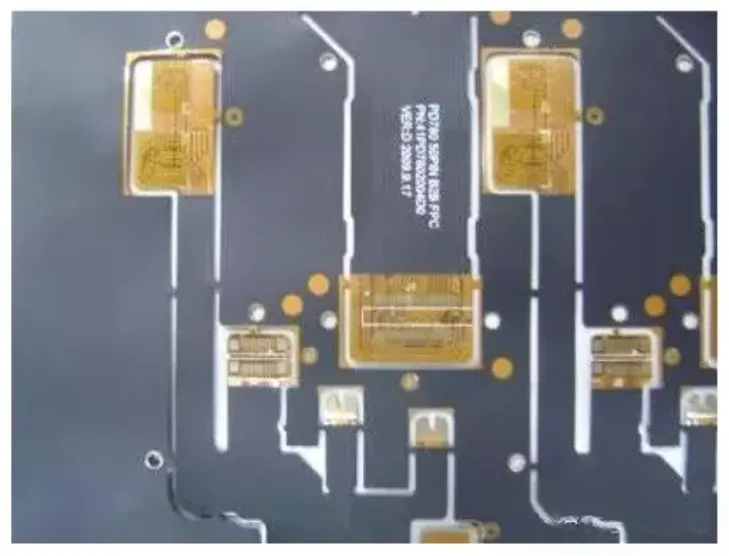
2. Methods for Separating Boards with Connecting Ribs
As shown in the figure below, this is an Flexible PCB connected using connecting ribs.
There are three methods for separating the boards:
- Manual separation using a utility knife or blade: Low precision and efficiency, but low cost.
- Die-cutting: Relatively low precision and short service life, but low cost and high efficiency.
- Steel die cutting. High precision, long service life, and high efficiency, but very high cost.
The appropriate cutting method should be selected based on product characteristics and order volume.
Why Flexible PCB SMT Is Different from Standard SMT
Although Flexible PCB (FPC) assembly follows the same fundamental Surface Mount Technology (SMT) workflow as conventional rigid PCB assembly—including solder paste printing, component placement, reflow soldering, inspection, and testing—the manufacturing requirements are significantly more demanding. Unlike rigid FR4 boards, flexible circuits are thin, bendable, and mechanically unstable.
These inherent material characteristics introduce unique challenges throughout the entire production process.
In conventional SMT production, the printed circuit board itself provides sufficient rigidity to maintain dimensional stability during printing, placement, and soldering.
Flexible PCBs, however, cannot maintain a flat and stable surface on their own. Without proper support, they are prone to deformation, stretching, warping, and movement, resulting in printing defects, component misalignment, and unreliable solder joints.
As electronic products continue to become smaller, lighter, and more functionally integrated, flexible circuits are increasingly used in smartphones, wearable devices, automotive electronics, medical equipment, aerospace systems, and other compact electronic products.
Consequently, flexible PCB assembly has evolved from a specialized manufacturing technique into a critical process for modern electronics production.
The key differences between flexible PCB SMT and conventional rigid PCB SMT are discussed below.
Lack of Rigidity
The most fundamental difference between flexible PCB assembly and rigid PCB assembly is the absence of structural rigidity.
A rigid PCB maintains its flatness throughout the SMT process, allowing it to move directly through automated production equipment with high positional accuracy.
Flexible PCBs, by contrast, are manufactured using polyimide (PI) or polyester (PET) substrates that can easily bend, twist, or wrinkle under external force.
Because of this flexibility, bare FPCs cannot be transported directly through SMT production lines. Any deformation during solder paste printing or component placement may cause registration errors, uneven solder paste deposition, or inaccurate component positioning.
To overcome this limitation, flexible PCBs must first be attached to dedicated carrier boards or fixtures before entering the production line. The carrier transforms the flexible circuit into a temporary rigid assembly, providing sufficient mechanical stability for automated processing.
The quality of fixture design directly influences production accuracy, assembly yield, and manufacturing efficiency.
Thermal Sensitivity
Flexible PCB materials exhibit significantly different thermal characteristics from traditional FR4 substrates.
Polyimide offers excellent flexibility and relatively high heat resistance; however, its thermal expansion behavior, thermal conductivity, and heat capacity differ considerably from rigid laminates. During reflow soldering, these differences affect temperature distribution across the board.
Excessive heating may lead to:
- Material blistering
- Delamination
- Adhesive degradation
- Excessive Z-axis expansion
- Permanent deformation of the flexible substrate
Unlike rigid PCBs, where thermal mass remains relatively uniform, flexible circuits often contain stiffeners, reinforcement plates, or locally thickened regions that absorb heat at different rates. Consequently, reflow profiles must be optimized specifically for each product rather than applying standard SMT temperature settings.
Lower peak temperatures, carefully controlled soak times, and gradual cooling are commonly employed to minimize thermal stress while maintaining solder joint reliability.
Dimensional Instability
Flexible substrates are considerably more susceptible to dimensional changes than rigid boards.
Temperature fluctuations, mechanical tension, fixture pressure, and material relaxation can all cause slight expansion or contraction during manufacturing.
Although these dimensional variations are often measured in only a few micrometers, they become increasingly significant as component pitches continue to shrink.
Modern flexible PCB assemblies frequently incorporate:
- Fine-pitch BGAs
- CSP packages
- QFNs
- 0201 and 01005 passive components
For these high-density assemblies, even small positional deviations may exceed acceptable process tolerances, leading to solder bridging, insufficient solder joints, component skew, or open circuits.
To minimize dimensional variation, manufacturers typically employ precision carrier boards, optical fiducial alignment systems, and tightly controlled environmental conditions throughout production.
Need for Specialized Carriers
Carrier boards are among the most critical enabling technologies in flexible PCB assembly.
Unlike rigid PCBs, which can be processed directly by SMT equipment, flexible circuits require dedicated carriers to provide mechanical support during every major manufacturing step, including:
- Solder paste printing
- SPI inspection
- Pick-and-place assembly
- Reflow soldering
- AOI inspection
- ICT and functional testing
An effective carrier board must satisfy several engineering requirements:
- High dimensional stability
- Excellent flatness
- Low thermal deformation
- Good heat dissipation
- Accurate positioning capability
- Long service life under repeated thermal cycling
Depending on production volume and product requirements, manufacturers commonly use engineering plastics, aluminum fixtures, silicone fixtures, or high-temperature magnetic carrier systems.
The fixture not only supports the flexible PCB mechanically but also directly influences print quality, placement accuracy, thermal uniformity, and overall manufacturing yield.
Support Requirements Throughout Production
Unlike rigid PCB assembly, where the substrate itself provides continuous mechanical support, flexible PCB manufacturing depends on external support throughout the entire production process.
Support requirements extend beyond fixture attachment alone. Every manufacturing stage requires process optimization specifically designed for flexible materials.
Examples include:
- Specialized polyurethane squeegees to compensate for slight height differences during solder paste printing.
- Carefully controlled placement forces to prevent deformation of thin polyimide substrates.
- Customized reflow temperature profiles to reduce thermal stress.
- Dedicated inspection fixtures that minimize movement during electrical testing.
- Controlled depaneling methods that prevent tearing or solder joint cracking.
Without comprehensive support throughout production, process stability deteriorates rapidly, resulting in higher defect rates and reduced manufacturing consistency.
Flexible PCB Assembly as a Coupled Manufacturing System
Traditional SMT process descriptions often present PCB assembly as a straightforward sequence of independent manufacturing steps: solder paste printing, component placement, reflow soldering, inspection, and testing.
While this simplified workflow is useful for understanding the production sequence, it does not accurately represent how modern flexible PCB assembly behaves in real manufacturing environments.
Flexible PCB assembly should instead be viewed as a coupled manufacturing system, in which every process stage continuously influences multiple downstream operations.
Rather than acting independently, printing, placement, thermal processing, fixture design, and inspection interact with one another throughout the production cycle.
For example, the design accuracy of a carrier board determines the flatness of the flexible substrate during solder paste printing. Paste volume uniformity subsequently affects component stability during placement. Placement accuracy influences solder paste deformation, which then alters wetting behavior during reflow soldering.
Finally, thermal expansion of both the fixture and the flexible substrate changes stress distribution within the solder joints, directly affecting long-term reliability.
This chain of interactions illustrates why optimizing a single process rarely guarantees improved product quality.
> Process Coupling and Tolerance Stack-Up
Every manufacturing stage introduces a small amount of process variation.
Examples include:
- Flexible PCB fabrication tolerance
- Carrier positioning accuracy
- Stencil manufacturing tolerance
- Solder paste volume variation
- Placement accuracy
- Reflow temperature fluctuation
- Material expansion during heating
Individually, each variation may remain within specification. However, these deviations accumulate throughout production in a phenomenon known as tolerance stack-up.
When the combined variation exceeds the allowable process window, manufacturing defects begin to appear, even though no individual process has technically failed.
> Interaction Between Printing, Placement, Reflow, and Fixtures
In flexible PCB assembly, manufacturing processes cannot be optimized independently.
Increasing stencil thickness may improve solder volume but simultaneously increase bridging risk.
Increasing placement force may improve component stability while deforming the flexible substrate.
Reducing peak reflow temperature may protect heat-sensitive components but reduce solder wetting quality.
Changing carrier material may improve thermal stability while altering heat transfer characteristics during reflow.
Successful process optimization therefore requires balancing the interaction between all manufacturing variables rather than maximizing the performance of individual processes.
> Why Defects Are Rarely Caused by a Single Process
Many common SMT defects—including tombstoning, solder bridging, component shifting, cold joints, and void formation—are often attributed to one obvious manufacturing step. In reality, these failures typically result from multiple interacting factors accumulated across the entire production process.
A slight fixture positioning error may combine with uneven solder paste deposition, minor placement offset, and localized thermal imbalance to produce a defect that only becomes visible after reflow soldering or even during field operation.
Consequently, advanced flexible PCB manufacturing increasingly relies on system-level process optimization, statistical process control (SPC), and closed-loop feedback from SPI, AOI, and production data to improve overall manufacturing stability.
Multi-Physics Nature of FPC Assembly
From an engineering perspective, flexible PCB assembly is not merely a mechanical manufacturing process. It is a multi-physics system in which mechanical behavior, thermal dynamics, material science, and process control continuously interact throughout production.
Understanding these interactions is essential for achieving high first-pass yield, minimizing defects, and ensuring long-term product reliability.
> Mechanical Behavior
Mechanical factors include substrate deformation, fixture rigidity, placement pressure, conveyor stability, and handling stress.
Because flexible circuits lack structural stiffness, even slight mechanical deformation can affect solder paste registration, component alignment, and solder joint geometry.
Proper fixture design and controlled handling are therefore fundamental to maintaining manufacturing consistency.
> Thermal Behavior
Thermal processes govern every stage of solder joint formation.
Heat transfer through the carrier board, flexible substrate, copper circuitry, and electronic components determines solder melting behavior, flux activation, intermetallic compound formation, and cooling characteristics.
Uniform temperature distribution is especially important for flexible assemblies because localized overheating can permanently damage the substrate while insufficient heating may result in incomplete solder wetting.
> Material Science
Material behavior significantly influences manufacturing quality.
The rheological properties of solder paste determine printability and stencil release.
Polyimide substrates expand differently from copper conductors.
Flux chemistry affects oxide removal and wetting.
Adhesives, stiffeners, and reinforcement materials each respond differently to repeated thermal cycling.
Understanding these material interactions enables engineers to optimize both manufacturing parameters and long-term product reliability.
> Process Control
Modern flexible PCB manufacturing increasingly relies on data-driven process control rather than isolated equipment optimization.
Inspection systems such as SPI, AOI, AXI, ICT, and FCT provide valuable feedback throughout production. By analyzing this information together with equipment parameters, manufacturers can continuously refine printing accuracy, placement precision, thermal profiles, and fixture performance.
This closed-loop manufacturing strategy reduces process variation, improves first-pass yield, minimizes rework, and produces more reliable flexible electronic assemblies.
Summary
When performing SMD placement on an Flexible PCB, precise positioning and securing of the Flexible PCB are critical. The key to proper securing lies in fabricating a suitable carrier board.
Other key steps include pre-baking, screen printing, component placement, and reflow soldering of the Flexible PCB. Clearly, the SMT process for Flexible PCBs is significantly more challenging than that for rigid PCBs.
Therefore, precise setting of process parameters is essential. At the same time, rigorous production process management is equally important.
Operators must strictly adhere to every provision in the SOP, while line engineers and IPQC personnel should intensify inspections to promptly identify anomalies on the production line, analyze the causes, and take necessary measures.
Only then can the defect rate on the Flexible PCB SMT production line be controlled within a few dozen PPM.