Rigid-Flex PCB for TWS Earbuds: Manufacturing Challenges and HDI Process Optimization
What is TWS (True Wireless Stereo)?
TWS (True Wireless Stereo) devices refer to systems in which a smart device connects to a master earbud, which then wirelessly transmits audio signals to a secondary earbud, enabling independent use of the left and right channels for stereo audio.
Traditional Bluetooth connection solutions can only connect a device to a single audio device.
Consequently, traditional wireless headphones are typically over-ear or neckband styles, with a wired connection between the left and right speakers.
A single master chip receives the audio signal and distributes it to the left and right speakers.
In contrast, TWS earbuds have no wired connection between the two audio devices and require a 1-to-2 connection when paired with a device.
Market Growth and Industry Impact
In 2016, Apple, as a pioneer in TWS earbuds, launched the first-generation AirPods, followed by the significantly upgraded AirPods Pro in 2019.
With the continuous expansion of product categories and ongoing improvements in user experience, TWS earbud shipments maintained a high growth rate in 2020.
According to statistics from Xuri Big Data and Zhiyan Consulting, the year-over-year growth rate of global TWS earbud shipments in the first quarter of 2020 exceeded 100%.
Looking ahead to the full year of 2020, TWS earbud shipments are expected to surpass 230 million units, with a year-over-year growth rate of 78.29%.
Among these, Chinese-brand TWS earbuds are set to capture over 70% of the global market share, thereby ushering in a new era of TWS 2.0 in China.
Benefiting from the widespread adoption and boom of TWS Bluetooth earbuds, the printed circuit board (PCB) industry has also gained a significant growth driver.
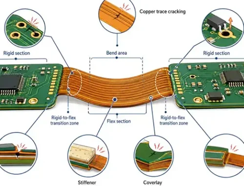
The PCB mainboards—a critical component of TWS Bluetooth earbuds—currently employ a rigid-flex (rigid-flexible) design.
Due to their lightweight, compact, flexible, and three-dimensional interconnection and assembly characteristics, they are highly favored by major manufacturers.
Technical Characteristics of Rigid-Flex PCB in TWS Devices
The rigid-flex solutions currently used in TWS Bluetooth earbud mainboards possess the following technical characteristics:
(1) 4-layer and 6-layer structures;
(2) 1st- and 2nd-order HDI;
(3) 0.025 mm flexible board + reinforcement; (4) On-pad design for the flexible board; (5) Assembly with multiple bending points.
This article takes a 6-layer, 2nd-order HDI rigid-flex board used in TWS Bluetooth earbuds as an example to provide a detailed analysis of its manufacturing challenges and quality control measures.
Product Overview
Product Architecture (see Figure 1)

Figure 1 Schematic diagram of a PCB stack up
Product Information (see Table 1)
| Layer Count | Stack Structure | Board Material / Coverlay | Prepreg | Minimum Line Width / Spacing | Minimum Via Hole | Finished Board Thickness | Surface Treatment | Reinforcement | Application Field |
|---|---|---|---|---|---|---|---|---|---|
| 6L | 2-stage HDI | ITEQ IF-2LD ITEQ IF-FC | EMC Low Flow pp | 63/63 μm (2.5/2.5 mil) | 0.2 mm | Rigid board: 0.5 ± 0.1 mm Flexible board: 0.18 ± 0.05 mm | Electroless Nickel Immersion Gold (ENIG) | SUS304 reinforcement | TWS Bluetooth Earphones |
Table 1. PCB Product Information
Process Flow
(1) L3-4 FPC Process: L3-4 panel cutting → Blind via drilling → Plasma cleaning → Blind via plating → L3-4 patterning → AOI → Browning → Cover film application → Laser windowing → Plasma cleaning
(2) Low-flow prepreg Process: Prepreg cutting → Backing adhesive application → Laser cutting → Trimming and forming
(3) Main Process: Pre-layout → L2-5 lamination → Copper reduction → Laser drilling → AOI → Blind via drilling → Via-filling plating → L2-5 patterning → AOI → Browning → Blind via plugging → Pre-layout → L1 -6 lamination → Copper reduction → Laser drilling → AOI → Blind via drilling → Via filling and plating → Outer layer patterning → AOI → Solder mask via filling → Solder mask → Text printing → Laser depth control → CNC (I) → Cover removal → Gold plating → CNC (II) → UV molding → Steel plate reinforcement → Electrical testing → FQC → Packaging
Analysis of Key Challenges
(1) Panelization Design: First, panel utilization must be at least 85%. HDI boards tend to be relatively thin, with the rigid section at 0.5 mm and the flexible section at 0.18 mm.
Furthermore, the flexible area is large and features multiple bends and folds. During surface treatment after opening the cover, the boards are prone to getting caught on the horizontal lines.
During final ET testing, insufficient support leads to numerous false contacts, which impacts efficiency;
(2) Fabrication Plan for Solder Pads in the Flexible Area: The solder pads are designed to be relatively small; evaluate appropriate process solutions based on the factory’s actual production capabilities;
(3) Panel Cutting Plan Evaluation: The typical thickness of HDI boards is around 100 mm.
Mechanically controlled depth cutting carries high risks; alternative cutting methods must be considered for connection points and the rigid-flex interface.
The flexible area is quite large, making standard pre-preg windowing unsuitable, as it is prone to delamination and board failure.
Since the flexible area includes solder pads, applying adhesive tape on the top side blocks the adhesive flow; the tape can contaminate the solder pads, and alignment issues and excessive adhesive overflow are common.
Process Analysis
Panel Layout Design
For this PCB, the rigid board is 0.5 ± 0.1 mm thick, and the FPC is 0.18 ± 0.05 mm thick.
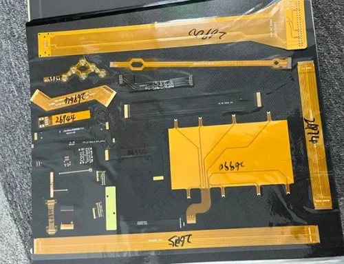
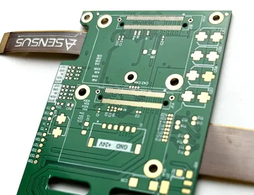
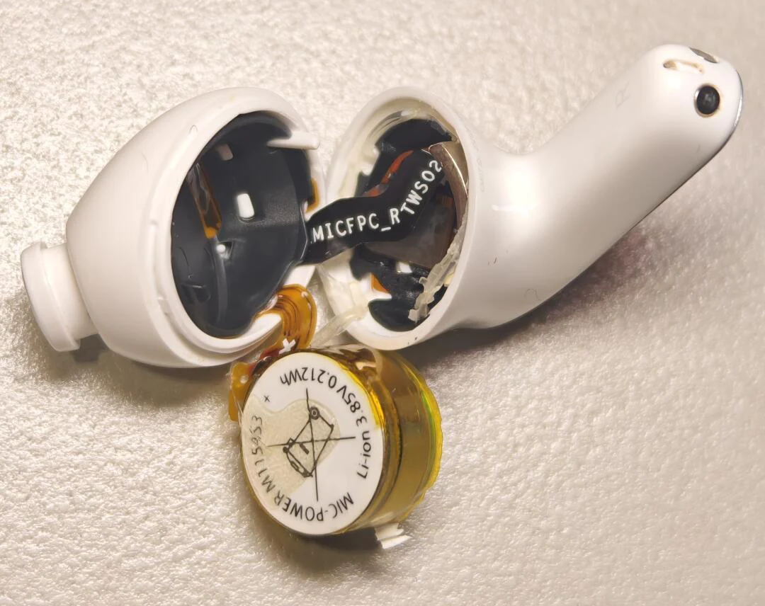
The crescent-shaped area of the rigid board consists of a 0.5 mm thick rigid substrate, while the remaining areas consist of a 0.18 mm thick flexible substrate (see Figure 2).
 and schematic diagram (right) of the TWS earbud mainboard")
Figure 2 Actual photo (left) and schematic diagram (right) of the TWS earbud mainboard
During actual production, the two panel layout schemes were compared as follows.
(1) In actual production, this scheme resulted in numerous issues.
When the board passed the horizontal line after milling, severe board jamming occurred due to insufficient support, leading to a high scrap rate.
Additionally, there were many false points during electrical testing, resulting in very low efficiency (see Figure 3).

Figure 3 Initial panel layout
(2) Optimized Panelization Design for Flexible Area PCB Manufacturability
The second scheme incorporates indirect connections between units via scrap areas, resulting in a smoother production flow (see Figure 4).
During panelization design, it is essential to consider not only utilization but also manufacturability.
For different circuit patterns—especially those with a high concentration of flexible areas—the distribution of connection points must be optimized to avoid direct connections between unit boards.
Sufficient scrap space should be maintained between any two unit boards to ensure adequate overall structural support.

Figure 4 Adjusted panel layout
Flexible Area Solder Pad Fabrication Plan
There are numerous solder pad designs in the flexible area, and no residual solder slag or foreign objects are permitted, as these would compromise soldering quality.
Based on actual factory conditions, a method involving laser windowing of the cover film was adopted. Laser parameters significantly affect the quality of the windowing;
if the cover film is not completely removed, it will severely impact the subsequent gold plating quality. In this test, different laser parameters were used for evaluation.
Test Equipment: Mitsubishi CO₂ Laser Machine
Procedure: Apply cover film to FPC → Laser windowing (CO₂) → Remove film → Gold plating
Parameters Used: Pulse width 2 μs, base energy 1 mJ, number of pulses 2. Following mass production, the surface quality of the connection pads after gold plating met specifications.
Design of the Decap Solution
(1) Back-Side Tape Application Process for Thin HDI Rigid-Flex PCB Manufacturing
Based on the product structure, the 2-layer, 6-layer HDI board has a dielectric thickness of approximately 0.10 mm. The flexible area includes a solder pad design.
Due to the relatively thin dielectric thickness, neither the traditional prepreg windowing method nor the conventional front-side tape application process can be used.
Considering these two factors, this product will be manufactured using a back-side tape application process.
The process flow for the back-side tape application is shown in Figure 5.

Figure 5 Back taping process flow
In the back-adhesive tape application process, two key points require special attention:
① Back-adhesive parameter settings: Temperature, pressure, and speed are critical parameters.
Improper settings can cause the film to wrinkle or peel off, which in turn prevents windowing in subsequent processes and results in product scrap. Current settings: Temperature 80°C, pressure 0.5 MPa, speed 3 m/min.
② UV cutting of the adhesive-backed product requires layered cutting with varying energy levels. First, use high energy to drill 3.175 mm semi-cured positioning holes, then use low energy to cut through the adhesive without penetrating the PP.
(2) Laser Depth-Controlled Processing for Rigid-Flex PCB Transition and Connection Areas
The finished board has a thickness of 0.5 mm, with L1-3 and L6-4 sections at 0.15 mm. Traditional mechanical depth-controlled blind milling easily damages the cover film; therefore, this board will adopt a laser depth-controlled solution.
Two critical areas require special attention: the interface between rigid and flexible sections and the connection points.
These areas require layered cutting with different energy levels.
At the rigid-flex transition points L1-3 and L6-4, the copper foil must be completely removed.
This requires extremely precise control to ensure easy panel opening without damaging the cover film. Based on the equipment’s capabilities, a minimum residual thickness of 0.05 mm is sufficient.
At the connection points L3 and L4, which feature a copper-clad design, the laser can be directed directly onto the copper surface; control at these locations is relatively straightforward.
Other Process Controls
See Table 2 for other process control requirements.
| No. | Process Name | Processing Description | Quality Requirements |
|---|---|---|---|
| 1 | FPC Process | RTR process | (1) No wrinkles allowed on the board surface (2) No exposure, edge lifting, burrs, or other defects |
| 2 | Lamination | Dedicated adhesive tape for lamination | No wrinkles or board jamming allowed on the board surface |
| 3 | Cover Film Lamination | Use transfer film for fitting; align according to unit alignment marks | Positional deviation must not exceed tolerance limits |
| 4 | Cover Film Pressing | Place green pressure pads and gray rubber pads above and below TPX for lamination | No offset or positional abnormalities allowed |
| 5 | UV Forming of AdhesiveTape | Reverse adhesive tape process | No bubbles, wrinkles, or peeling allowed |
| 6 | Pre-Arrangement | Use Teflon adhesive tape to assist thermal melting; time: 60 s | Thermal melting area must not show carbonization. For adhesive tape units connected to the carrier board by only a half-cured sheet, the remaining half-cured sheets must be fixed with adhesive tape |
| 7 | Lamination Pressing | Place three-in-one + aluminum sheets above and below; aluminum sheets close to the board; lamination program: Low flow | / |
| 8 | Outer Layer Dry Film | High-low difference adjustment, pressure rolling; pressure 6 kg; speed 1.2 m/min or 60 pressure rolls | No bubbles or wrinkles allowed |
| 9 | Laser Profiling Control | No energy-layer cutting allowed at soft-hard interface edges or connection positions | 1. No damage to cover film at soft-hard interface edges; cutting depth tolerance ≤ 50 μm 2. No damage at connection bridge positions |
| 10 | Cover Opening in Soft Board Area | Assign dedicated personnel; use specialized cover-opening tools | (1) No scratches, burrs, oil stains, etc. (2) No residual adhesive or semi-cured sheet powder allowed on pad surfaces |
| 11 | Electrical Testing | Needle-bed testing | / |
| 12 | Reinforcement Lamination | Refer to reinforcement lamination instruction drawings | No misalignment or omission allowed; X-board also requires lamination |
| 13 | FQC | Inspect according to soft-hard combined board finished product inspection standards | / |
Table 2. Other Process Control Requirements
Summary
Based on the manufacturing process of this TWS Bluetooth earbud HDI rigid-flex board, the key process control requirements are summarized as follows:
(1) For different circuit patterns, especially those with a high concentration of flexible areas, the placement of connection points must avoid direct connections between module blocks.
Sufficient scrap space must be maintained between any two modules to ensure adequate structural support;
(2) For FPC solder pad fabrication, control the laser ablation energy to ensure the cover film is completely removed and the solder pad surface quality is excellent;
(3) For laminating prepregs in thin HDI boards, use a reverse-taping process to facilitate opening the cover; UV cutting requires layered cutting with different energy levels;
(4) For opening the cover, a laser depth-control solution is employed. Two critical areas require special attention: the rigid-flex interface and the connection points.
These areas require layered cutting with different energy levels.
During the design phase, the copper foil at the rigid-flex interface must be completely removed.
This requires extremely precise laser energy to ensure easy opening without damaging the cover film. Based on equipment capabilities, a minimum residual thickness of 0.050 mm is sufficient.