LCD/OLED Module Basics—An Introduction to FPC Raw Material Manufacturing
Flexible PCB are a foundational technology in modern electronics, enabling compact, lightweight, and highly reliable interconnections between components in devices such as smartphones, automotive control units, medical instruments, and wearable electronics.
Unlike traditional rigid PCBs, Flexible PCB are built on flexible polymer substrates, allowing them to bend, fold, and conform to tight spatial constraints without compromising electrical performance.
Understanding how an FPC is manufactured is crucial for comprehending both its structural reliability and its potential applications in advanced electronic systems.
The production of a double-sided FPC involves a tightly controlled sequence of precision processes—from copper foil lamination and micro-scale drilling to chemical copper deposition, circuit patterning, and final electrical testing.
Each stage directly influences the circuit’s conductivity, mechanical durability, and long-term stability.
This section provides a systematic overview of the complete manufacturing workflow for double-sided Flexible PCB, breaking down the 11 core process steps and explaining how each contributes to forming a functional, high-precision flexible circuit ready for integration into electronic assemblies.
What Is an FPC?
FPC: Flexible Printed Circuit
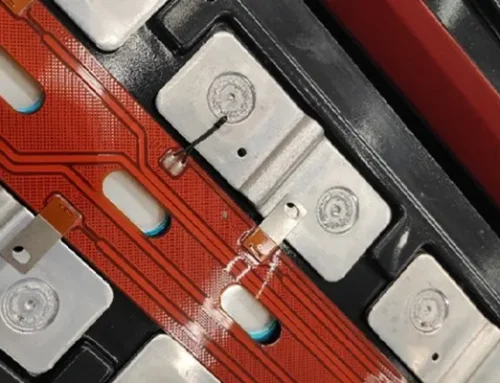
1. In the module configuration shown below, the component marked by the red dashed box is the FPC.

Figure 1. The FPC is marked with red dashed lines
2. Individual components are generally loaded onto trays; black and white trays are commonly used for this purpose.

Figure 2. Single-unit FPC Tray disk loading
FPC Manufacturing Process Flow
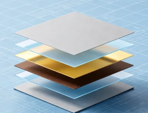
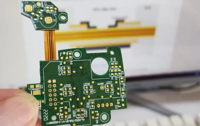
Based on double-sided FPC boards, verify the FPC production process.

Figure 3 Double-sided FPC board
A total of 11 main processes (which vary significantly from one manufacturer to another).
① Copper Cladding → ② Die-Cutting → ③ Drilling → ④ Through-Hole Copper Plating → ⑤ Circuit Formation → ⑥ Coverlay Laminating → ⑦ Curing → ⑧ Surface Treatment → ⑨ Filler Lamination and Punching → ⑩ Electrical Testing → ⑪ Inspection, Packaging, and Shipping

Figure 4: Overall FPC production process flow
Production Processes
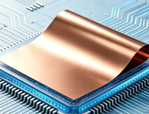
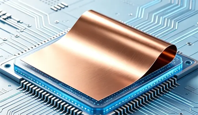
1. Process: Copper Foil Lamination
Laminate the copper foil onto the base film coated with adhesive.

Figure 5 Copper Sheet
2. Process: Cutting
During the production process, the material is cut according to the product size.

Fig 6 Cutting
3. Process: Drilling
Includes 2 main pieces of equipment: NC machine, drilling
① NC machine:
By manually adjusting the product length, a pin punching machine is used to punch and position holes in the product, facilitating machining on the 6-axis NC drilling machine.

Figure 7 NC equipment
② Drilling:
Using six-axis CNC drilling equipment, through-holes are mechanically drilled into the copper surface using drill bits of various diameters according to preset drilling coordinates.
This is followed by a copper plating process to ensure electrical continuity between the two copper surfaces.

Figure 8 Drilling
4. Process: Copper Plating of Holes
Includes two main processes: black hole treatment, copper plating, and visual inspection.
① Black Hole Treatment:
Through chemical treatment, carbon particles are adsorbed onto the surface of the product’s bonding layer to form a conductive layer.

Figure 9. Copper plating at holes
② Copper Plating:
Using electrochemical principles, electrolytic copper is deposited on the surface of the copper and the inner walls of the holes to ensure electrical conductivity throughout the structure.
③ Visual Inspection: Conduct a visual inspection of the finished products to identify any defective items.

Figure 10 Visual inspection
5. Process: Circuit Formation
Includes three main processes: circuit pretreatment, dry film lamination, and exposure.
① Circuit Pretreatment: A low-concentration hydrochloric acid solution is used to clean the copper surface of foreign matter and deposits, keeping the surface clean to reduce defects.
② Dryfilm Lamination:

Fig 11: Dryfilm Lamination
③ Exposure: The process in which ultraviolet light strikes the exposed film and causes it to harden.

Fig12: Exposure
6. Process: Coverlay Lamination
Includes two main pieces of equipment: Coverlay Test Lamination and Coverlay Final Lamination
① Coverlay Test Lamination:
Using a test lamination machine, the material and the product are temporarily bonded together based on the principles of low temperature, low pressure, and precise positioning. At this stage, the two are not yet firmly bonded together.

Fig13: Coverlay
② Coverlay Laminating:
Using the high temperature and high pressure of a laminating machine to melt the adhesive, thereby tightly bonding the materials and the finished product together.

Fig14: Coverlay Laminating
7. Process: Curing
Place the pressed product in an oven and use the oven’s sustained high temperature to fully cure the interlayer adhesive and set the product’s shape.
8. Process: Surface Treatment
Includes 2 main pieces of equipment: OSP, chemical nickel-gold plating, and electroplated nickel-gold
① OSP: Utilizes a chemical reaction to form a thin film on the exposed copper surface, which, at a certain temperature, protects the copper surface from oxidation.
② Chemical nickel-gold plating, electroplated nickel-gold.
The process of forming a uniform, dense, and well-bonded metal layer on a copper surface using electroplating or chemical plating.
9. Process: Patch Material Bonding and Stamping
Includes 2 main pieces of equipment: patch material bonding and stamping.
① Patch Material Bonding:
The workpiece is positioned by aligning the locating pins on the fixture with the locating holes on the workpiece.
② Stamping:
Using the operating principles of stamping presses and dies, the external shape of the product is formed by punching away excess material to achieve the final shape required by the customer.
10. Process: Electrical Inspection
The probes on the electrical test fixture make contact with the gold-plated (tin or copper) areas on the product to test the circuit performance (e.g., short circuits, open circuits, etc.).
11. Step: Final Inspection, Packing, and Shipping
Summary
In summary, the manufacturing of double-sided Flexible Printed Circuits (Flexible PCB) is a highly integrated and precision-driven process that combines mechanical fabrication, chemical treatment, and electrical engineering principles.
From copper foil lamination and fine drilling to through-hole copper plating, circuit pattern formation, and final surface finishing, each step plays a critical role in ensuring electrical integrity and structural reliability.
The subsequent processes—including coverlay lamination, curing, stamping, and electrical testing—further enhance the FPC’s durability, insulation performance, and assembly accuracy.
These tightly controlled stages collectively transform raw laminated materials into functional, flexible interconnection systems capable of meeting the demanding requirements of modern electronic applications.
Overall, the 11-step manufacturing workflow reflects the complexity and precision of FPC production, where every detail directly impacts final product quality.
A clear understanding of this process not only highlights the technical sophistication behind flexible circuits but also provides essential insight for quality control, design optimization, and advanced electronic manufacturing.