Optimization of Differential Impedance in FPCB Using Mesh Copper Reference Layer
With the rapid development of high-frequency, high-speed electronic devices, signal integrity (SI) design for flexible printed circuit boards (FPCBs) faces increasingly stringent challenges.
The signal reflection loss and crosstalk levels of transmission lines directly determine impedance stability, and their tolerances typically need to be controlled within ±10%.
When a copper mesh is used as the reference plane for transmission lines, fluctuations in the proportion of solid copper area cause significant variations in transmission line impedance, thereby affecting the overall performance of the circuit board.
To address this issue, this paper establishes a parametric model using the 3D electromagnetic simulation software CST to analyze the influence of copper mesh orientation on impedance fluctuations.
A mesh rotation-based impedance optimization scheme is proposed, which significantly improves impedance consistency.
Factors Affecting Strip-Line Differential Impedance
Parallel-coupled differential line structures are commonly used for critical signal transmission in high-speed circuits.
Compared to single-ended transmission lines, differential lines offer the advantages of being less susceptible to noise interference and providing better resistance to crosstalk and abrupt discontinuities.
The formulas for strip-line single-ended impedance Z0 and strip-line differential impedance Zdiff are:

Where:
- W is the trace width;
- S is the trace spacing;
- H is the dielectric thickness;
- T is the copper thickness;
- εr is the relative permittivity of the dielectric.
The impedance of a stripline is primarily influenced by trace width, trace spacing, dielectric thickness, copper thickness, and the relative permittivity of the dielectric.
- Trace width W is inversely proportional to impedance;
- Reducing trace spacing S enhances coupling effects and lowers impedance;
- Increasing dielectric thickness H raises impedance; increasing copper thickness T lowers impedance;
- The dielectric constant of the dielectric material directly affects the impedance value.
Etching precision in the manufacturing process introduces impedance deviations.
Dielectric layer uniformity in the manufacturing process introduces impedance deviations.
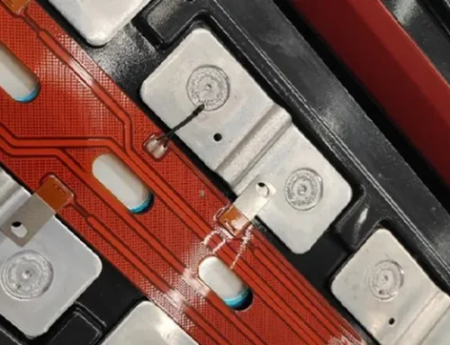
The integrity of the reference plane alters the circuit path. Solid copper and copper mesh form the reference plane.
The altered circuit path affects the impedance characteristics.
Layer Stackup Design and Strip-Line Impedance Design
For standard FPCB layer stackup design and strip-line impedance design, the stackup materials are shown in Table 1.
The impedance requirements for the strip-line are as follows: the 100 Ω signal line is located on the middle layer (L2), with L1 copper and L3 copper serving as reference planes.
| Layer Structure | Thickness (μm) | Material Model |
|---|---|---|
| CVL | 32 | (DuPont) HXC1220 |
| L1 Copper | 12 | |
| PI | 25 | (Taiflex) 2LPSR1003JC |
| Adhesive | 25 | (Arisawa) AE15-25KA |
| L2 Copper | 12 | |
| PI | 25 | (Taiflex) 2FPDR1003JC |
| L3 Copper | 12 | |
| CVL | 32 | (DuPont) HXC1220 |
Table 1. Common FPCB Lamination Materials
Simulation of Strip-Line Impedance for Solid Copper and Mesh Copper Reference Layers
A solid copper model was created in CST software, as shown in Figure 1.

Figure 1 Simulation of a differential pair on a solid copper reference plane
The simulation results show that the impedance value is close to 100 Ω when the line width is 28 μm and the line spacing is 122 μm;
However, this line width does not meet the minimum line width requirements of conventional manufacturing processes.
Next, the solid copper traces for L1 and L3 were replaced with a copper grid with a line width of 100 μm and a line spacing of 200 μm.
The copper grid forms a 45° angle with the impedance lines. The two differential lines are centered symmetrically about the diagonal of the copper grid.
Figure 2 shows the configuration.

Figure 2: Simulation of differential lines on a copper reference plane
With a line width of 38 μm and a spacing of 112 μm, the impedance is close to 100 Ω, and this line width generally meets the requirements of standard manufacturing processes.
Comparative experiments examine solid copper and mesh copper. The stack-up thickness and material selection remain the same.
A mesh copper design effectively increases the line width. The increased line width meets the same impedance targets.
This approach is more conducive to ensuring process stability for the line width.
Furthermore, the smaller the proportion of solid copper in the mesh copper, the wider the line width becomes; therefore, the appropriate mesh copper dimensions can be designed based on actual requirements.
Effect of Differential Line Impedance on the Relative Position of Grid Copper
In practical FPCBs, most are high-density circuit boards with multiple sets of impedance lines in adjacent positions.
In this simulation, the grid copper design remains unchanged with a line width of 100 μm, a line spacing of 200 μm, and a differential pair width of 38 μm.
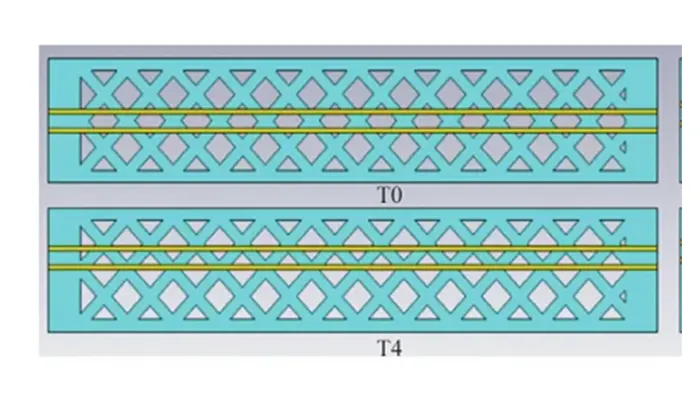
We compare the simulated impedance values corresponding to different differential pair spacings, different angles between the grid lines and the impedance lines, and the position of the shifted differential pairs.
The T0 state centers the differential pair symmetrically relative to the grid copper diagonal. The T1 state shifts the differential pair upward by 25 μm. The T2 state shifts the differential pair upward by 50 μm.
The T3 state shifts the differential pair upward by 75 μm. The T4 state shifts the differential pair upward by 100 μm. The T5 state shifts the differential pair upward by 125 μm. The T6 state shifts the differential pair upward by 150 μm.
The simulation models for the T0, T2, T4, and T6 states are shown in Figure 3.
")
Figure 3: Differential line simulation model of a copper reference plane (with the impedance line and plane at a 45° angle)
Table 2 compares the impedance values for seven different states.
› Effect of Differential Pair Position and Coupling on Impedance
The simulation results show that after the differential pair is shifted, the proportion of solid copper in the copper mesh directly beneath the differential pair varies, leading to changes in impedance.
In actual production, it is difficult to precisely control impedance consistency.
The spacing between differential pairs also affects impedance values; reducing the spacing between the two lines reduces the coupling effect.
In Table 2, one differential pair has a spacing of 112 μm, referred to as loose coupling; the other has a spacing of 62 μm, referred to as tight coupling.
A comparison of the impedance fluctuation ranges for loose and tight coupling reveals that, because the relative positions of the two lines in tight coupling are closer, their impedance values are more similar.
Consequently, the fluctuation range of the coupled differential impedance is smaller, which is more conducive to controlling the consistency of the grid copper impedance lines.
› Optimization of Grid Angle for Improved Impedance Consistency
To address the issue of the relative position of the grid reference layer affecting the impedance values of the loosely coupled differential lines, the angle between the grid lines and the impedance lines was adjusted from 45° to 35°.
As shown in the simulation results in Table 2, at this grid angle, the difference in actual copper area between the positive and negative sides of the differential lines is small, and the impedance variation is minimal.
The minimum impedance is 108.025 Ω, and the maximum impedance is 108.145 Ω, with the impedance variation controlled within 3%, effectively improving the impedance consistency of the FPCB.
| Mesh Copper (Line Width/Line Spacing) | Differential Line (Line Width/Line Spacing) | T0 | T1 | T2 | T3 | T4 | T5 | T6 |
|---|---|---|---|---|---|---|---|---|
| 100/200 μm, angle 45° | 38/112 μm (Loose) | 101.275 | 102.530 | 107.323 | 112.717 | 115.616 | 114.598 | 110.261 |
| 100/200 μm, angle 45° | 38/62 μm (Dense) | 97.891 | 98.139 | 99.927 | 101.238 | 102.697 | 102.563 | 100.808 |
| 100/200 μm, angle 35° | 38/112 μm | 108.111 | 108.057 | 108.085 | 108.003 | 108.145 | 108.042 | 108.025 |
Table 2. Differential Line Impedance Values of Mesh Copper Reference Layer
Conclusion
Based on simulation comparison data, this paper draws several important conclusions:
- Under identical stackup and material parameters, when the target impedance is the same, a mesh copper reference layer design requires wider trace widths than a solid copper reference layer, making it easier to meet FPCB manufacturing requirements.
- Under identical stackup and material parameters, when the impedance lines form a 45° angle with the grid, the impedance fluctuation range of tightly coupled differential pairs is smaller than that of loosely coupled differential pairs.
- Under the same stackup and material parameters, when the angle between the impedance lines and the grid is adjusted from 45° to 35°, the amplitude of impedance fluctuations can be reduced by more than 50%.
This optimization scheme provides an effective approach for improving impedance consistency control in high-frequency FPCBs.