PCB Hole Wall Quality Inspection: Methods, Criteria, and Defect Fixes
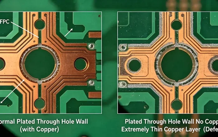

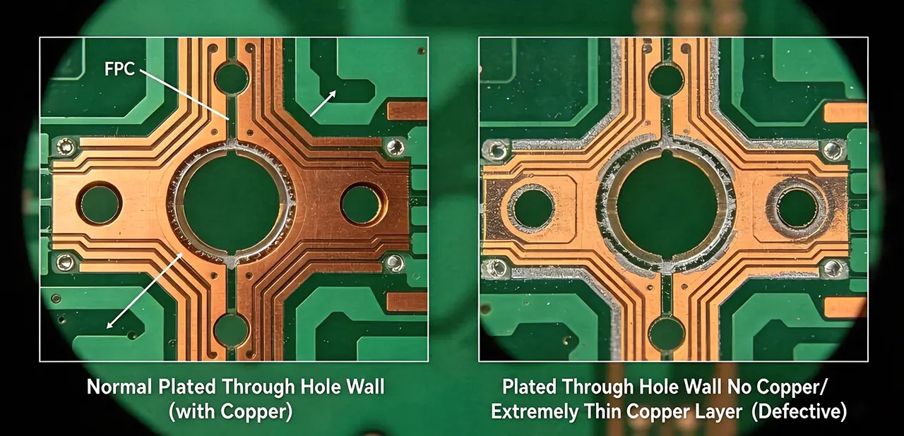
PCB hole wall quality inspection is the set of visual, mechanical, and electrical checks used to confirm that the copper plating inside a drilled or laser-formed hole is continuous, well bonded, and thick enough to survive thermal cycling. A complete program combines AOI screening, backlight testing, copper thickness measurement, and destructive cross-section analysis evaluated against IPC-6012 and IPC-A-600 acceptance criteria.
It sounds procedural \u2014 and it is \u2014, but the payoff is simple: a board that passes hole wall inspection does not open up in the field. Below is how the inspection actually works, what inspectors look for, which defects appear most often, and how to fix the process when they do.
What PCB Hole Wall Quality Inspection Actually Covers
“Hole wall quality” is shorthand for several distinct characteristics, each with its own measurement method:
| Characteristic | What is being verified |
|---|---|
| Plating continuity | No voids, gaps, or unplated areas in the copper barrel |
| Copper thickness | Average and minimum barrel copper within spec |
| Adhesion/bond strength | Copper-to-dielectric and copper-to-inner-layer connection |
| Etchback or negative etchback | Correct resin removal before plating |
| Surface condition | No resin smear, fiber protrusion, or drill debris |
| Barrel geometry | No cracks, pullaway, nailheading, or barrel distortion |
A panel can pass one of these checks and fail another. That is why single-method programs \u2014 a backlight test alone, for example \u2014 miss escapes that only a cross-section would catch.
Why It Matters More Than Most Engineers Expect
The hole wall carries current between layers and, in multilayer and HDI designs, it is the most thermally stressed feature on the board. Holes accumulate:
- Drill-induced mechanical stress from the drilling operation itself
- Chemical and thermal stress during desmear, plating, and lamination
- Z-axis expansion stress during assembly reflow
- Field thermal cycling over the product’s service life
A thin or voided barrel can pass electrical test at the factory and fail months later in the field. For automotive, medical, aerospace, and IPC Class 3 applications, hole wall defects are a documented reliability risk, not a cosmetic issue.
Inspection Methods: From Fast Screening to Definitive Proof
1. Visual and AOI screening
Automated optical inspection flags surface-level anomalies around the hole entry and exit: missing copper, annular ring defects, burrs, and gross plating gaps. Modern systems add laser scanning and machine vision to grade hole quality at high throughput, but AOI cannot see inside the barrel. It is a filter, not a verdict.
2. Backlight test (light-through test)
The backlight test is the fastest non-destructive check on plating coverage. A sample is placed over a light source and viewed from above; light passing through the dielectric reveals voids, thin spots, and poor coverage as bright pinpoints. Results are reported as a percentage or as a bounded void area. It is an excellent process-monitoring tool for plating bath control, but it is qualitative and sample-based.
3. Cross-section microsection (the reference method)
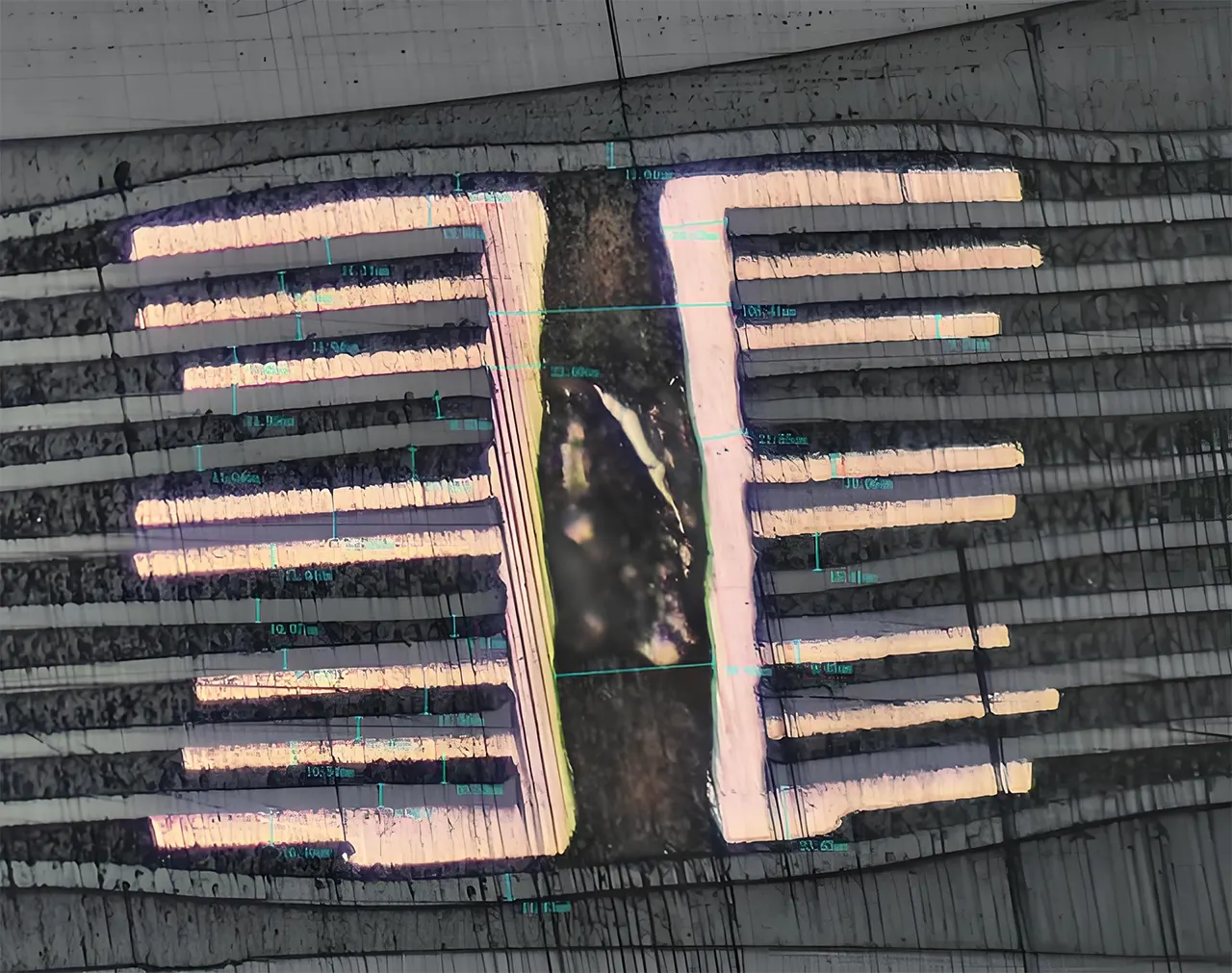
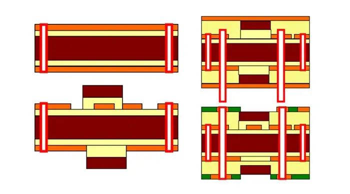
Cross section of hole
Microsectioning is the definitive check, and the one most customer specifications name explicitly. A plated sample is potted, ground, polished, and examined under a metallurgical microscope at 100x to 500x magnification, following IPC-TM-650 microsectioning methods. Inspectors measure barrel copper at three points around the wall, look for voids, cracks, and separation, and confirm etchback and inner-layer connection.
Where you cut matters. Cross-sections should be taken through the hole center and, for high-reliability work, at multiple holes across the panel \u2014 including the worst-case holes: smallest drill, highest aspect ratio, panel edge.
4. Copper thickness measurement
Barrel copper is measured two ways: non-destructively near the hole on the surface (XRF or micro-resistance) as a process indicator, and directly on the microsection for the true barrel value. Mature programs track average thickness, minimum thickness, and Cpk across a plating lot rather than a single number.
5. Thermal stress, IST, and HAST
Thermal stress testing (solder float or reflow simulation), interconnect stress testing (IST), and highly accelerated stress testing (HAST) drive cracks and latent voids to the surface. These are the checks that reveal whether plating is genuinely bonded or merely thick enough to pass electrical test today.
6. X-ray and CT scanning
X-ray verifies hole registration, barrel alignment, and plating in blind vias. Micro-CT adds cross-sectional imaging without destroying the sample, which is useful for failure analysis and for HDI structures where a physical microsection is hard to target.
7. Automated and AI-assisted evaluation
Increasingly, plating labs use machine vision to classify hole wall images and to correlate AOI and microsection data with plating bath parameters. That data can then feed back into the process \u2014 the same principle behind AI-driven flexible circuit board production optimization on high-volume lines, where hole counts are high and hold times are short.
Acceptance Criteria: What “Good” Looks Like
Exact limits come from the applicable specification \u2014 IPC-6012 (rigid), IPC-6013 (flexible), IPC-A-600 for visual interpretation \u2014 and from the customer drawing, which usually wins in a conflict. Commonly applied targets include:
| Parameter | Class 2 (typical) | Class 3 (typical) | How it is measured |
|---|---|---|---|
| Average barrel copper | ~20 µm | ~25 µm | Microsection |
| Minimum barrel copper | Defined per spec | Higher and tighter | Microsection |
| Voids in barrel | Small, bounded allowable area | Essentially none in the plated barrel | Backlight + microsection |
| Barrel cracks | Not allowed | Not allowed | Microsection |
| Etchback / negative etchback | Defined range per drawing | Defined, tighter range | Microsection |
| Plating adhesion | No separation after thermal stress | No separation, stricter | Thermal stress + microsection |
Treat that table as orientation, not as a substitute for the current revision of the standard. Specifications change, and Class 3 nuance is where audits are won and lost.
Common Hole Wall Defects and Their Root Causes
| Defect | What it looks like | Typical root cause |
|---|---|---|
| Plating void | Gap in barrel copper, bright spot under backlight | Bath chemistry out of range, weak throwing power, trapped air, contaminated barrel |
| Barrel crack | Fracture across the copper after thermal stress | High Z-axis expansion, thin copper, brittle plating, excessive thermal stress |
| Resin smear | Smearing film over inner-layer copper | Worn drill bit, wrong drilling parameters, inadequate desmear |
| Fiber protrusion | Glass fibers exposed at the wall | Aggressive drilling, insufficient etchback, weak desmear chemistry |
| Nailheading | Inner-layer copper deformed into a wedge | Drill wear, excessive feed rate, unsupported stack |
| Hole wall pullaway | Copper separated from dielectric | Poor adhesion, thermal mismatch, contamination |
| Incomplete desmear | Resin residues in the barrel | Insufficient plasma or permanganate desmear, poor rinse |
Process Controls That Actually Prevent Defects
Inspection finds problems; process control prevents them. The highest-leverage controls are:
Drilling. Bit wear is the single largest variable. Log hole count per bit, replace on schedule, and confirm spindle runout and stack-up rigidity. Different board types need different strategies, and the same logic that governs PCB drilling techniques laser mechanical quality applies to hole wall integrity, because entry and exit conditions set up everything downstream.
Desmear and etchback. Set the etchback target with the customer, then verify it on every plating lot. Under-desmear leaves resin; over-etchback damages inner-layer connection and can create wicking paths.
Plating chemistry and throwing power. Aspect ratio drives throwing power requirements. High-aspect-ratio holes need bath optimization for both composition and agitation, and thickness should be tracked with SPC rather than a pass/fail reading. On flexible copper-clad laminate, substrate preparation directly affects plating uniformity; see this carbon-coated film FCCL copper plating evaluation for how substrate choice changes the result.
Sampling plan. Define how many holes, from how many panels, and how often. First-article microsections plus a documented periodic frequency beats ad-hoc cutting every time.
Data feedback. Cross-section results should update drilling and plating parameters, not just sit in a report. The closed-loop approach described in AI-driven flexible circuit board production optimization is a good model.
Extra Considerations for Flex and Rigid-Flex Boards
Flexible and rigid-flex products stress hole walls differently. Polyimide absorbs more moisture, the dielectric is thinner and more compliant, and laser-drilled microvias have a different wall morphology than mechanically drilled holes. Points to watch:
- Microvias and laser drilling. Wall quality depends on pulse energy and taper control; flex PCB micro-drilling hole quality covers the parameter trade-offs in detail.
- Blind and buried structures. blind slot multilayer flexible PCB manufacturing is where registration, dielectric thickness, and wall coverage interact most tightly.
- Rigid-flex transitions. The flex-to-rigid boundary concentrates mechanical stress, so inspection should include the transition zone; rigid-flex PCB manufacturing process optimization covers the process side.
- Assembly-level effects. Solder and laser-welded joints can mask or amplify underlying barrel issues, so laser welding FPCB joint quality is worth reviewing alongside hole wall data for boards that pass through laser soldering.
Building a Repeatable Inspection Workflow
1. Define acceptance criteria from the customer drawing and the applicable IPC standard.
2. Qualify the process with first-article microsections: barrel copper, voids, etchback, adhesion.
3. Set a production sampling frequency by hole type and aspect ratio.
4. Run backlight testing and copper thickness measurement as ongoing process monitors.
5. Trigger thermal stress or IST whenever plating parameters change.
6. Log every result against the panel lot and the plating bath condition.
7. Review defects monthly and feed corrective actions back into drilling and plating.
FAQ
What is PCB hole wall quality inspection?
It is the combination of checks \u2014 visual/AOI, backlight, copper thickness, thermal stress, and destructive microsection \u2014 that verify the copper plating inside a drilled or laser-formed hole is continuous, adhered, and thick enough for the product’s thermal and mechanical requirements. Acceptance criteria come from IPC-6012 / IPC-6013, IPC-A-600, and the customer drawing.
Is a backlight test enough to qualify hole wall plating?
No. Backlight testing is fast, non-destructive, and excellent for monitoring plating coverage trends, but it is qualitative and cannot measure barrel copper thickness, detect hairline cracks, or verify etchback. Cross-section microsectioning remains the reference method and is usually the method named in customer specifications for qualification.
How thick should copper plating be in a PCB hole wall?
For rigid boards, IPC-6012 commonly calls for roughly 20 \u00b5m average (Class 2) to 25 \u00b5m average (Class 3) of copper in the hole wall, plus a defined minimum. Flexible boards follow IPC-6013. Always confirm against the current revision of the standard and the customer drawing, because reliability classes and special applications can be stricter.
How often should microsections be taken?
Typically on first article for each new job or panel design, after any plating or drilling parameter change, and then on a defined periodic sampling frequency during production \u2014 often per plating lot or per shift, depending on reliability class and customer requirements. Worst-case holes (smallest diameter, highest aspect ratio) should be prioritized.
What causes a hole wall plating void?
The most common causes are plating bath chemistry out of range, insufficient throwing power for the hole’s aspect ratio, trapped air or bubbles, contamination or incomplete desmear on the barrel surface, and unstable agitation. Voids frequently appear first near the hole center, which is why centerline cross-sections matter.
Do flexible PCBs need different hole wall criteria?
Yes. Polyimide-based flex and rigid-flex boards use thinner dielectrics, absorb more moisture, and rely more on laser-drilled microvias, so wall morphology differs from mechanically drilled rigid boards. IPC-6013 applies, and inspection should explicitly cover laser-drilled microvias and the rigid-flex transition zone.
Bottom Line
PCB hole wall quality inspection is only as good as the loop it feeds. A backlight test that never changes a bath parameter, or a microsection report that never reaches the drilling floor, costs money without buying reliability. GekunFlex builds flexible and rigid-flex boards with documented microsection, backlight, copper thickness, and thermal stress data behind the hole wall. Send your stack-up and reliability class, and we will review the inspection plan that fits it.
Related Posts
- Improve PCB Micro-Drill Performance on Flex Boards — Related article
- Laser Welding FPCB Quality Guide — Related article
- Optimizing Blind Slot Multilayer Flexible PCB Manufacturing — Related article
- pcb-drilling-techniques-guide — Related article
- AI-Driven Optimization of FPCB Production Processes — Related article